How to make textolite with your own hands. Alignment of the upper and lower photomasks on the surfaces of the workpiece
Tahiti! .. Tahiti! ..
We have not been to any Tahiti!
We are well fed here!
© Cartoon cat
Introduction with digression
How were boards made before in domestic and laboratory conditions? There were several ways - for example:
- drew future conductors with penguins;
- engraved and cut with cutters;
- they glued adhesive tape or electrical tape, then the drawing was cut out with a scalpel;
- the simplest stencils were made, followed by drawing with an airbrush.
The missing elements were drawn with drawing pen and retouched with a scalpel.
It was a long and laborious process, requiring remarkable artistic abilities and accuracy from the “drawer”. The thickness of the lines hardly fit into 0.8 mm, there was no repetition accuracy, each board had to be drawn separately, which greatly hindered the release of even a very small batch printed circuit boards (hereinafter - PP).
What do we have today?
Progress does not stand still. The times when radio amateurs painted PP with stone axes on mammoth skins have sunk into oblivion. The appearance on the market of publicly available chemistry for photolithography opens up completely different prospects for the production of PP without metallizing holes at home.
Let's take a quick look at the chemistry used to make PP today.
Photoresist
You can use liquid or film. We will not consider film in this article due to its scarcity, the difficulties of rolling onto the PP and more Low quality output printed circuit boards.
After analyzing market offers, I settled on POSITIV 20 as the optimal photoresist for home PCB production.
Purpose:
POSITIV 20 is a photosensitive varnish. It is used in small-scale production of printed circuit boards, engravings on copper, when carrying out work related to the transfer of images to various materials.
Properties:
High exposure characteristics ensure good contrast of transferred images.
Application:
It is used in areas related to the transfer of images to glass, plastics, metals, etc. in small-scale production. The method of application is indicated on the bottle.
Characteristics:
Color: blue
Density: at 20°C 0.87 g/cm3
Drying time: at 70°C 15 min.
Consumption: 15 l/m2
Maximum photosensitivity: 310-440nm
The instructions for the photoresist say that you can store it at room temperature and it is not subject to aging. Strongly disagree! You need to store it in a cool place, for example, on the bottom shelf of the refrigerator, where the temperature is usually maintained at + 2 ... + 6 ° C. But in no case do not allow negative temperatures!
If you use photoresists that are sold "in bulk" and do not have opaque packaging, care must be taken to protect from light. It is necessary to store in complete darkness and at a temperature of +2 ... + 6 ° C.
Enlightener
Similarly, I find TRANSPARENT 21, which I use all the time, to be the most suitable illuminator.
Purpose:
Allows direct transfer of images onto surfaces coated with POSITIV 20 photosensitive emulsion or other photoresist.
Properties:
Gives transparency to paper. Provides UV light transmission.
Application:
For quick transfer of contours of drawings and diagrams to the substrate. Allows you to significantly simplify the process of reproduction and reduce time s e costs.
Characteristics:
Color: transparent
Density: at 20°C 0.79 g/cm3
Drying time: at 20°C 30 min.
Note:
Instead of plain paper with an illuminator, you can use a transparent film for inkjet or laser printers, depending on what we will print the photomask on.
Photoresist Developer
There are many different solutions for developing photoresist.
It is advised to develop with a solution of "liquid glass". His chemical composition: Na 2 SiO 3 *5H 2 O. This substance has a huge number of advantages. The most important thing is that it is very difficult to overexpose PP in it - you can leave PP for a non-fixed time. The solution almost does not change its properties with temperature changes (there is no risk of decomposition with increasing temperature), it also has a very long shelf life - its concentration remains constant for at least a couple of years. The absence of the problem of overexposure in the solution will make it possible to increase its concentration in order to reduce the time of manifestation of PP. It is recommended to mix 1 part concentrate with 180 parts water (a little over 1.7 g of silicate in 200 ml of water), but it is possible to make the mixture more concentrated so that the image develops in about 5 seconds without the risk of surface damage due to overexposure. If it is not possible to purchase sodium silicate, use sodium carbonate (Na 2 CO 3) or potassium carbonate (K 2 CO 3).
I have not tried either the first or the second, so I will tell you what I have been showing without any problems for several years now. I use an aqueous solution of caustic soda. For 1 liter cold water- 7 grams of caustic soda. If there is no NaOH, I use a KOH solution, doubling the concentration of alkali in the solution. The development time is 30-60 seconds with the correct exposure. If, after 2 minutes, the pattern does not appear (or appears weakly), and the photoresist begins to wash off from the workpiece, it means that the exposure time has been chosen incorrectly: you need to increase it. If, on the contrary, it quickly appears, but both the illuminated and unexposed areas are washed off, either the concentration of the solution is too high or the quality of the photomask is low (ultraviolet passes freely through the “black”): you need to increase the print density of the template.
Copper pickling solutions
Excess copper from printed circuit boards is etched using various etchants. Among people doing this at home, ammonium persulfate, hydrogen peroxide + hydrochloric acid, copper sulfate solution + table salt are often common.
I always poison with ferric chloride in glassware. When working with the solution, you need to be careful and attentive: if it gets on clothes and objects, they remain rust spots, which are difficult to remove with a weak solution of citric (lemon juice) or oxalic acid.
We heat the concentrated solution of ferric chloride to 50-60 ° C, immerse the workpiece in it, gently and effortlessly drive the glass rod with a cotton swab at the end over areas where copper is worse etched - this achieves more even etching over the entire area of the PCB. If the speed is not forced to equalize, the required duration of etching increases, and this eventually leads to the fact that in areas where copper has already been etched, etching of the tracks begins. As a result, we do not have what we wanted to get. It is highly desirable to provide continuous mixing of the pickling solution.
Chemistry for removing photoresist
What is the easiest way to wash off the already unnecessary photoresist after etching? After repeated trial and error, I settled on ordinary acetone. When it is not there, I wash it off with any solvent for nitro paints.
So, we make a printed circuit board
Where does a high quality PCB start? Correctly:
Creating a high quality photomask
For its manufacture, you can use almost any modern laser or inkjet printer. Given that we are using a positive photoresist in this article, where copper should remain on the PCB, the printer should draw black. Where there should be no copper, the printer should not draw anything. Highly important point when printing a photomask: it is required to set the maximum ink watering (in the settings of the printer driver). The more black the shaded areas are, the more likely you are to get a great result. Color is not needed, a black cartridge is enough. From that program (we will not consider programs: everyone is free to choose for himself - from PCAD to Paintbrush), in which the photomask was drawn, we print on a regular sheet of paper. The higher the resolution when printing and the better the paper, the higher the quality of the photomask will be. I recommend at least 600 dpi, the paper should not be very thick. When printing, we take into account that the side of the sheet on which the paint is applied, the template will be placed on the PP blank. If done otherwise, the edges of the PCB conductors will be blurry, fuzzy. Let the paint dry if it was an inkjet printer. Next, we impregnate TRANSPARENT 21 paper, let it dry and ... the photomask is ready.
Instead of paper and an illuminator, it is possible and even very desirable to use a transparent film for laser (when printing on a laser printer) or inkjet (for inkjet printing) printers. Please note that these films have unequal sides: only one working. If you're using laser printing, I highly recommend doing a "dry run" of a sheet of film before printing - just run the sheet through the printer, simulating printing, but not printing anything. Why is this needed? When printing, the fuser (oven) will heat up the sheet, which will inevitably lead to its deformation. As a result - an error in the geometry of the PP at the output. In the manufacture of double-sided PP, this is fraught with a mismatch of layers with all the consequences ... And with the help of a “dry” run, we will warm up the sheet, it will deform and be ready for printing a template. When printing, the sheet will pass through the oven for the second time, but the deformation will be much less significant - it has been tested repeatedly.
If the PCB is simple, you can draw it manually in a very convenient program with a Russified interface - Sprint Layout 3.0R (~650 KB).

On the preparatory stage it is very convenient to draw not too bulky electrical circuits in the also Russified program sPlan 4.0 (~ 450 KB).

This is how ready-made photomasks printed on an Epson Stylus Color 740 printer look like:


We print only in black, with the maximum watering of the dye. Material - transparent film for inkjet printers.
Preparing the PCB surface for photoresist application
For the production of PP are used sheet materials coated with copper foil. The most common options are with a copper thickness of 18 and 35 microns. Most often, for the production of PP at home, sheet textolite (a fabric pressed with glue in several layers), fiberglass (the same thing, but epoxy compounds are used as glue) and getinax (pressed paper with glue) are used. Less often - sittal and polycor (high-frequency ceramics - used extremely rarely at home), fluoroplastic (organic plastic). The latter is also used for the manufacture of high-frequency devices and, having very good electrical characteristics, can be used anywhere and everywhere, but its use is limited by a high price.
First of all, you need to make sure that the workpiece does not have deep scratches, burrs and areas affected by corrosion. Next, it is desirable to polish the copper to a mirror. Polishing is not particularly zealous, otherwise we will erase without that thin layer copper (35 microns) or, in any case, we will achieve different thickness copper on the surface of the workpiece. And this, in turn, will lead to different speed Etching: Erases faster where it is thinner. Yes and more thin conductor on the board - not always good. Especially if it is long and a decent current will flow through it. If the copper on the workpiece is of high quality, without sins, then it is enough to degrease the surface.
Deposition of photoresist on the surface of the workpiece
We place the board on a horizontal or slightly inclined surface and apply the composition from an aerosol package from a distance of about 20 cm. Remember that the most important enemy in this case is dust. Every particle of dust on the surface of the workpiece is a source of problems. To create a uniform coating, spray the spray in a continuous zigzag motion, starting from the top left corner. Do not overspray as this causes unwanted streaks and results in uneven coating thickness requiring longer exposure times. Summer high temperature environment re-treatment may be required, or the aerosol may need to be sprayed from a shorter distance to reduce evaporative losses. When spraying, do not tilt the can strongly - this leads to an increased consumption of propellant gas and, as a result, the aerosol can stops working, although there is still photoresist in it. If you get unsatisfactory results with spray coating of photoresist, use spin coating. In this case, the photoresist is applied to a board mounted on a rotating table with a drive of 300-1000 rpm. After finishing the coating, the board should not be exposed to strong light. By the color of the coating, you can approximately determine the thickness of the applied layer:
- light gray blue - 1-3 microns;
- dark gray blue - 3-6 microns;
- blue - 6-8 microns;
- dark blue - more than 8 microns.
On copper, the color of the coating may have a greenish tinge.
The thinner the coating on the workpiece, the better the result.
I always apply photoresist on a centrifuge. In my centrifuge, the rotation speed is 500-600 rpm. Fastening should be simple, clamping is done only at the ends of the workpiece. We fix the workpiece, start the centrifuge, spray on the center of the workpiece and observe how the photoresist spreads over the surface in a thin layer. By centrifugal forces, excess photoresist will be thrown off the future PCB, so I highly recommend providing a protective wall so as not to turn workplace in a pigsty. I use an ordinary pan, in the bottom of which a hole is made in the center. The axis of the electric motor passes through this hole, on which a mounting platform in the form of a cross of two aluminum rails is installed, along which the ears of the workpiece clamp “run”. The ears are made of aluminum corners clamped on the rail with a wing nut. Why aluminum? Small specific gravity and, as a consequence, less runout when the center of mass of rotation deviates from the center of rotation of the axis of the centrifuge. The more precisely the workpiece is centered, the less beating will be due to the eccentricity of the mass and the less effort will be required to rigidly fasten the centrifuge to the base.
Photoresist applied. Let it dry for 15-20 minutes, turn the workpiece over, apply a layer on the second side. We give another 15-20 minutes to dry. Do not forget that direct sunlight and fingers on the working sides of the workpiece are unacceptable.
Tanning of photoresist on the workpiece surface
We place the workpiece in the oven, gradually bring the temperature to 60-70 ° C. At this temperature we maintain 20-40 minutes. It is important that nothing touches the surfaces of the workpiece - only touches of the ends are allowed.
Alignment of the upper and lower photomasks on the surfaces of the workpiece
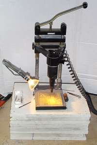
On each of the photomasks (upper and lower) there should be marks, according to which 2 holes must be made on the workpiece - to match the layers. The farther apart the marks, the higher the alignment accuracy. I usually place them diagonally across the templates. Using these marks on the workpiece, using a drilling machine, we drill two holes strictly at 90 ° (the thinner the holes, the more accurate the alignment - I use a 0.3 mm drill) and combine the templates along them, not forgetting that the template must be applied to the photoresist the side that was printed on. We press the templates to the workpiece with thin glasses. It is preferable to use quartz glasses - they transmit ultraviolet better. Plexiglas (plexiglass) gives even better results, but it has an unpleasant scratching property, which will inevitably affect the quality of the PP. At small sizes PP can use the transparent cover from the packaging of the CD. In the absence of such glasses, ordinary window glass can also be used, increasing the exposure time. It is important that the glass is even, ensuring that the photomasks fit evenly on the workpiece, otherwise it will not be possible to obtain high-quality track edges on the finished PCB.

A blank with a photomask under plexiglass. We use the box from under the CD.
Exposure (flare)
The time required for exposure depends on the thickness of the photoresist layer and the intensity of the light source. POSITIV 20 photoresist varnish is sensitive to ultraviolet rays, the maximum sensitivity falls on the area with a wavelength of 360-410 nm.
It is best to expose under lamps whose radiation range is in the ultraviolet region of the spectrum, but if you do not have such a lamp, you can use ordinary powerful incandescent lamps by increasing the exposure time. Do not start illumination until the illumination from the source stabilizes - it is necessary that the lamp warms up for 2-3 minutes. The exposure time depends on the thickness of the coating and is usually 60-120 seconds when the light source is located at a distance of 25-30 cm. The glass plates used can absorb up to 65% of ultraviolet, so in such cases it is necessary to increase the exposure time. Best results are achieved with transparent plexiglass plates. When using a photoresist with long term exposure time may need to be doubled - remember: photoresists are subject to aging!
Examples of using various sources Sveta:


UV lamps
We expose each side in turn, after the exposure we let the blank stand for 20-30 minutes in a dark place.
Development of the exposed workpiece
We develop in a solution of NaOH (caustic soda) - see the beginning of the article for details - at a solution temperature of 20-25 ° C. If there is no manifestation up to 2 minutes - small about exposure time. If it appears well, but useful areas are also washed off - you are too smart with the solution (the concentration is too high) or the exposure time is too long with this radiation source or the photomask is of poor quality - insufficiently saturated printed black color allows ultraviolet light to illuminate the workpiece.
When developing, I always very carefully, without effort, “roll” a cotton swab on a glass rod in those places where the exposed photoresist should be washed off - this speeds up the process.
Washing the workpiece from alkali and residues of exfoliated exposed photoresist
I do this under a faucet—ordinary tap water.
Retanning photoresist
We place the workpiece in the oven, gradually raise the temperature and hold at a temperature of 60-100 ° C for 60-120 minutes - the pattern becomes strong and solid.
Checking the development quality
For a short time (for 5-15 seconds) we immerse the workpiece in a solution of ferric chloride heated to a temperature of 50-60 ° C. Rinse quickly with running water. In places where there is no photoresist, intensive etching of copper begins. If a photoresist is accidentally left somewhere, carefully mechanically remove it. It is convenient to do this with a conventional or ophthalmic scalpel, armed with optics (soldering glasses, loupes a watchmaker, loop a on a tripod, microscope).
Etching
We pickle in a concentrated solution of ferric chloride with a temperature of 50-60°C. It is desirable to ensure continuous circulation of the pickling solution. We gently “massage” badly etched places with a cotton swab on a glass rod. If the ferric chloride is freshly prepared, the pickling time usually does not exceed 5-6 minutes. We wash the workpiece with running water.


Board etched
How to prepare a concentrated solution of ferric chloride? We dissolve FeCl 3 in slightly (up to 40 ° C) heated water until it ceases to dissolve. Filter the solution. Store in a dark, cool place in an airtight non-metallic package - in glass bottles, For example.
Removing unwanted photoresist
We wash off the photoresist from the tracks with acetone or a solvent for nitro-paints and nitro-enamels.
Hole drilling
It is advisable to select the diameter of the point of the future hole on the photomask in such a way that it would be convenient to drill later. For example, with the required hole diameter of 0.6-0.8 mm, the dot diameter on the photomask should be about 0.4-0.5 mm - in this case, the drill will be well centered.
It is advisable to use drills coated with tungsten carbide: drills made of high speed steels wear out very quickly, although steel can be used for drilling large diameter single holes (greater than 2 mm), since tungsten carbide coated drills of this diameter are too expensive. When drilling holes with a diameter of less than 1 mm, it is better to use a vertical machine, otherwise your drills will break quickly. If drilling hand drill- distortions are inevitable, leading to inaccurate joining of holes between layers. The downward movement on a vertical drilling machine is the most optimal in terms of tool loading. Carbide drills are made with a rigid (i.e. the drill exactly fits the diameter of the hole) or with a thick (sometimes called "turbo") shank having standard size(usually 3.5 mm). When drilling with carbide-coated drills, it is important to firmly fix the PCB, since such a drill, when moving up, can lift the PCB, skew the perpendicularity and tear out a piece of the board.
Small diameter drills are usually inserted into either a collet chuck (various sizes) or a three-jaw chuck. For precise fixation, clamping in a three-jaw chuck is not the best the best way, and a small drill size (less than 1 mm) quickly grooves in the jaws, losing good hold. Therefore, for drills with a diameter of less than 1 mm, it is better to use a collet chuck. Just in case, get an extra set containing spare collets for each size. Some inexpensive drills are made with plastic collets - throw them away and buy metal ones.
To obtain acceptable accuracy, it is necessary to properly organize the workplace, that is, firstly, to ensure good lighting drilling boards. For this you can use halogen lamp, attaching it on a tripod to be able to choose a position (illuminate right side). Second, raise work surface about 15 cm above the countertop for better visual control of the process. It would be nice to remove dust and chips during the drilling process (you can use a regular vacuum cleaner), but this is not necessary. It should be noted that the dust from fiberglass generated during drilling is very caustic and, if it comes into contact with the skin, causes skin irritation. And finally, when working, it is very convenient to use the foot switch of the drilling machine.
Typical hole sizes:
- vias - 0.8 mm or less;
- integrated circuits, resistors, etc. - 0.7-0.8 mm;
- large diodes (1N4001) - 1.0 mm;
- contact pads, trimmers - up to 1.5 mm.
Try to avoid holes with a diameter of less than 0.7 mm. Always keep at least two spare drills 0.8 mm or less, as they always break at the very moment when you urgently need to order. Drills 1mm and larger are much more reliable, although it would be nice to have spare ones for them. When you need to make two identical boards, you can drill them at the same time to save time. In this case, it is necessary to very carefully drill holes in the center of the pad near each corner of the PCB, and for large boards, holes located close to the center. Lay the boards on top of each other and, using the 0.3mm centering holes in two opposite corners and the pins as pegs, secure the boards against each other.
If necessary, you can countersink holes with drills of a larger diameter.
Copper tinning on PP
If you need to irradiate the tracks on the PCB, you can use a soldering iron, soft low-melting solder, alcohol-rosin flux and coaxial cable braid. With large volumes, they are tinned in bathtubs filled with low-temperature solders with the addition of fluxes.
The most popular and simple melt for tinning is the low-melting alloy "Rose" (tin - 25%, lead - 25%, bismuth - 50%), the melting point of which is 93-96 ° C. The board is placed with tongs under the level of the liquid melt for 5-10 seconds and, having taken it out, it is checked whether the entire copper surface is covered evenly. If necessary, the operation is repeated. Immediately after removing the board from the melt, its residues are removed either with a rubber squeegee or by sharp shaking in a direction perpendicular to the plane of the board, while holding it in the clamp. Another way to remove residues of the Rose alloy is to heat the board in an oven and shake it. The operation can be repeated to achieve a mono-thick coating. To prevent oxidation of the hot melt, glycerin is added to the tinning tank so that its level covers the melt by 10 mm. After the end of the process, the board is washed from glycerin in running water. Attention! These operations involve working with installations and materials that are under the influence of high temperature, therefore, to prevent burns, it is necessary to use protective gloves, goggles and aprons.
The tin-lead tinning operation proceeds similarly, but more heat melt limits the scope this method in handicraft production.
Do not forget to clean the board from flux after tinning and degrease thoroughly.
If you have a large production, you can use chemical tinning.
Applying a protective mask
Application operations protective mask exactly repeat everything that was written above: we apply a photoresist, dry, tan, center the photomasks of the masks, expose, develop, wash and tan again. Of course, we skip the steps with checking the quality of development, etching, removing photoresist, tinning and drilling. At the very end, we tan the mask for 2 hours at a temperature of about 90-100 ° C - it will become strong and hard, like glass. The formed mask protects the surface of the PCB from external influences and protects against theoretically possible short circuits during operation. It also plays an important role in automatic soldering - it does not allow the solder to “sit down” on neighboring sections, closing them.
That's it, the double-sided printed circuit board with the mask is ready.
I had to make PP in this way with the width of the tracks and the step between them up to 0.05 mm (!). But this is a piece of jewelry. And without special efforts you can make PP with a track width and a step between them of 0.15-0.2 mm.
I did not apply a mask to the board shown in the photographs - there was no such need.


Printed circuit board in the process of mounting components on it
And here is the device itself, for which the software was made:

This is a cellular telephone bridge that allows you to reduce the cost of services by 2-10 times mobile communications- for the sake of this it was worth messing with the PP;). The PCB with soldered components is in the stand. Previously, there was an ordinary charger for mobile phone batteries.
Additional Information
Hole plating
At home, you can even metallize holes. For this inner surface holes are treated with a 20-30% solution of silver nitrate (lapis). Then the surface is cleaned with a squeegee and the board is dried in the light (you can use a UV lamp). The essence of this operation is that under the action of light, silver nitrate decomposes, and inclusions of silver remain on the board. Next, copper is chemically precipitated from the solution: copper sulphate (copper sulfate) - 2 g, sodium hydroxide - 4 g, ammonia 25% - 1 ml, glycerin - 3.5 ml, formalin 10% - 8-15 ml, water - 100 ml. The shelf life of the prepared solution is very short - you need to prepare immediately before use. After the copper is deposited, the board is washed and dried. The layer is obtained very thin, its thickness must be increased to 50 microns by galvanizing.
Electroplating solution for copper plating:
For 1 liter of water, 250 g of copper sulfate (copper sulfate) and 50-80 g of concentrated sulfuric acid. The anode is a copper plate suspended parallel to the part to be coated. The voltage should be 3-4 V, current density - 0.02-0.3 A / cm 2, temperature - 18-30 ° C. The lower the current, the slower the metallization process, but the better the resulting coating.

Fragment of the printed circuit board, where the metallization is visible in the hole
Homemade photoresists
Photoresist based on gelatin and potassium bichromate:
First solution: pour 15 g of gelatin into 60 ml boiled water and leave to swell for 2-3 hours. After swelling of the gelatin, place the container on water bath at a temperature of 30-40°C until the gelatin is completely dissolved.
The second solution: in 40 ml of boiled water, dissolve 5 g of potassium dichromate (chromic peak, bright orange powder). Dissolve in low ambient light.
Pour the second into the first solution with vigorous stirring. Add a few drops to the resulting mixture with a pipette ammonia until a straw color is obtained. The photographic emulsion is applied to the prepared board in very low light. The board dries to "tack" at room temperature in complete darkness. After exposure, wash the board in low diffused light in warm running water until the untanned gelatin is removed. To better evaluate the result, you can stain areas with unremoved gelatin with a solution of potassium permanganate.
Advanced Homemade Photoresist:
First solution: 17 g of wood glue, 3 ml of an aqueous solution of ammonia, 100 ml of water, leave to swell for a day, then heat in a water bath at 80 ° C until completely dissolved.
Second solution: 2.5 g potassium dichromate, 2.5 g ammonium dichromate, 3 ml aqueous ammonia solution, 30 ml water, 6 ml alcohol.
When the first solution has cooled to 50°C, pour the second solution into it with vigorous stirring and filter the resulting mixture ( this and subsequent operations must be carried out in a darkened room, sunlight is unacceptable!). The emulsion is applied at a temperature of 30-40°C. Further - as in the first recipe.
Photoresist based on ammonium dichromate and polyvinyl alcohol:
We prepare the solution: polyvinyl alcohol - 70-120 g / l, ammonium dichromate - 8-10 g / l, ethyl alcohol - 100-120 g / l. Avoid bright light! It is applied in 2 layers: the first layer - drying for 20-30 minutes at 30-45°C - the second layer - drying for 60 minutes at 35-45°C. Developer - 40% solution ethyl alcohol.
Chemical tinning
First of all, the board must be decapitated in order to remove the formed copper oxide: 2-3 seconds in a 5% hydrochloric acid solution, followed by rinsing in running water.
It is enough to simply carry out chemical tinning by immersing the board in an aqueous solution containing tin chloride. The release of tin on the surface of the copper coating occurs when immersed in a solution of tin salt, in which the copper potential is more electronegative than the coating material. A change in the potential in the desired direction is facilitated by the introduction of a complexing additive, thiocarbamide (thiourea), into the tin salt solution. Solutions of this type have the following composition (g/l):
Among the listed solutions, solutions 1 and 2 are the most common. Sometimes, as a surfactant for the 1st solution, it is proposed to use Progress detergent in an amount of 1 ml / l. The addition of 2-3 g/l of bismuth nitrate to the 2nd solution leads to the precipitation of an alloy containing up to 1.5% bismuth, which improves the solderability of the coating (prevents aging) and greatly increases the shelf life before soldering the components of the finished PP.
To preserve the surface, aerosol sprays based on fluxing compositions are used. After drying, the varnish applied to the surface of the workpiece forms a strong, smooth film that prevents oxidation. One of the popular substances is "SOLDERLAC" from Cramolin. Subsequent soldering is carried out directly on the treated surface without additional varnish removal. In especially critical cases of soldering, the varnish can be removed with an alcohol solution.
Artificial tinning solutions deteriorate over time, especially when exposed to air. Therefore, if you have large orders infrequently, then try to cook immediately a large number of enough solution to tin the desired amount of PP, and store the remaining solution in a closed container (bottles of the type used in the photograph are ideal, which do not allow air to pass through). It is also necessary to protect the solution from contamination, which can greatly degrade the quality of the substance.
In conclusion, I want to say that it is still better to use ready-made photoresists and not bother with metallizing holes at home - you still won’t get great results.
Many thanks to the candidate of chemical sciences Filatov Igor Evgenievich for advice on chemistry-related matters.
I also want to express my gratitude Igor Chudakov.
At home. It is difficult for a beginner to navigate even in a world where you need a lot of things to make a simple board, so I will try to briefly and clearly tell you how to make a board is not expensive and simple. So, let's get down to the step-by-step instructions.
Instructions for the manufacture of printed circuit boards
Board drawing

Foil textolite

Ferric chloride on sale

Ferric chloride in crystals

Tray for etching

Tray for etching boards

Finished homemade board
- 1. You will need textolite, or fiberglass for the future board.
- 2. Cut out carefully, having previously marked the right dimensions from a piece, with small allowances, I make the workpiece approximately 1 cm larger, so it’s better to press especially small boards later, plus another part will go to sawing, grinding, and so on.
- 3. After the desired piece is cut off, we take a larger sandpaper and go through it along the edges so that there are no nicks that would interfere with pressing.
- 4. We grind the very surface of the foil with fine sandpaper so that it shines.
- 5. We go through and wash off the copper dust after grinding with a solvent 646 .
- 6. We are waiting for it to dry from the previous process, we print on a laser printer on glossy paper what is from the program, having previously drawn the tracks and layouts that are required.
- 7. We check what is printed, it is necessary to print with a higher resolution of the printer, which is only possible, and with toner saving turned off.
- 8. We apply the workpiece, I glue the edges with paper masking tape, and iron with a good effort for 2-3 minutes with a heated iron at a temperature of 180-220 degrees, depending on what melting point the toner has.
- 9. We wait until it cools down, do not touch anything at all - it should cool down slowly by itself. There is no need to put the board in the freezer, under the fan, outside the window, in the water, the toner should dry as it should, and only so securely grab. It takes time, usually 10-15 minutes and you need to be patient.
- 10. We take a bath of suitable sizes, pour about half of the usual cool water, put the whole thing with paper after cooling, wait a couple of minutes and start removing and scrubbing the paper, we must act carefully, I do everything with my hands without improvised means.
- 11. We take the same bath made of plastic, not metal for sure, dilute ferric chloride (1-2 tablespoons per 200-300 grams of water) with heated water 40-50 degrees, wait until the mixture is stirred properly and stops actively bubbling.
- 12. We glue the board with stationery double-sided tape to a piece of foam plastic from the packaging material, send it to the voyage, shaking it a little and letting it get wet well so that it sinks a little, and wait, it takes some time.
- 13. While the solution is fresh, the printed circuit board is usually etched for 15-30 minutes, after which we pull out the board when the tracks are shaped as in the program where they were printed from - and rinse under the tap from the remnants of ferric chloride.
- 14. We take cotton wool and acetone - remove the toner that covered the tracks, clean it well so that there is no trace left.
- 15. We grind the handkerchief with fine sandpaper from oxides and wash it again with a solvent.
- 16. Everything can be covered with mortar LTI-120 and start tinkering.
- 17. After the board is tinned, let it cool down and drill.
- 18. We carry out grinding reverse side, trimming the edges and giving an aesthetically beautiful and desired view and form of payment.
Any electronic device requires connecting together a bunch of parts. Of course, you can solder the device on the circuit board, but at the same time there is a high risk of making a bunch of mistakes, and the device itself will look very dumb. Wires sticking out in all directions will be appreciated only by lovers of trash design. Therefore, we will make a printed circuit board!
And to make it easier for you, I made a video lesson on the topic of manufacturing printed circuit boards using the method laser iron aka LUT.
A full cycle, from preparing the board from a piece of textolite, to drilling and tinning.
Printed circuit boards are made of foil insulating material (getinax, fiberglass, fluoroplast). A metal foil is firmly glued to one of the sides of the sheet of insulating material, which makes it possible to obtain printed conductors of any shape in the future. They are a strip of foil connecting the leads of two or more parts mounted on a printed circuit board in accordance with circuit diagram radio engineering device.
What is required for the manufacture of printed circuit boards?
0) Drawing of the printed circuit board in electronic form.
1) Laser printer for printing an imprint of the future board. It is desirable that the printer has the possibility of a direct path - printing with minimal paper bending. I have Samsung ML1520. Print to the maximum, without any toner saving!
2) Foil textolite.
3) Photo paper for inkjet printing Lomond 120g/m glossy, one-sided with improved coating. Also good results on Lomond 230g/m glossy paper.
4) Brush for suede with metal + plastic pile (optional)
5) Acetone
6) Nulevka skin
The shape of the conductors, their number and mutual arrangement are determined by the device diagram, the elements used, as well as the experience of a radio amateur developing a printed circuit board drawing.
It must be remembered that the drawings are developed for the installation of well-defined types of elements. If the types of some elements are different (for example, instead of capacitors of the K50-6 type, capacitors of the K53-4 type with a different pin arrangement are used), then the board drawing will have to be changed accordingly.
Most often, radio amateurs use foil fiberglass of the STF brand or foil getinaks of the GF brand for the manufacture of a printed circuit board. Getinaks in comparison with fiberglass has slightly worse characteristics, but it is quite suitable for the vast majority of amateur radio structures. When working with getinax, use fusible solders (POSK-50, POS-40, POS-61), since the foil can easily peel off when the printed conductors overheat during soldering.
Foil materials produced by industry have different thickness. Typically, a material with a thickness of 1.5 mm is used. But in cases where the board is large and massive elements need to be installed on it, a material with a thickness of 2-2.5 mm is used.
If you do not have ready-made foil material at your disposal, you can make it yourself.
Cut out a workpiece from a getinax 1.5-2 mm thick to fit the future board, and from a sheet of copper foil (its thickness should be in the range of 0.05-0.1 mm) - a plate of the same size. Sand the surfaces to be bonded with fine-grained sandpaper, clean them of dust and degrease with acetone or gasoline. Apply a current layer of BF-2 glue on the getinaks and foil and dry it for an hour at room temperature, then apply a second layer of glue and dry for 30 minutes. After that, put the foil on the getinaks and roll it with a hard roller from the middle to the edges. Place the workpiece processed in this way under a press or in a vise and hold for 2-3 days.
Place the workpiece between two metal plates (lay additional cardboard on the side of the foil) and firmly squeeze the entire package.
Drawing a printed circuit board
Prepare an auxiliary drawing of the printed circuit board from the side of the printed conductors on a scale of 1: 1, mark the centers of the future holes with dots.
Glue the design to the foil with a few drops of rubber glue. With the help of a center punch, with light blows of a small hammer, alternately transfer the centers of all future holes to the foil,
Keep the punch perpendicular to the surface of the board, otherwise the marking will be inaccurate. Before this operation, do not sand the foil so that the marks left by the center punch are more noticeable.
Remove the drawing from the workpiece and drill holes. It is best to do this on a drilling machine, since the holes for the outputs of the parts have 0 0.8 -1 mm. You can also use an electric drill. To do this, clamp the workpiece in a vise through cardboard or getinax spacers with foil towards you. Sitting on a chair, place the elbow of your left hand on a workbench, place an electric drill in your palm, and right hand hold the drill by the handle.
Adjust the drill feed in the horizontal plane with the coordinated movements of both hands. As you drill holes, change the position of the workpiece, at the end of the work, check whether all the holes have been drilled.
Sand the foil with fine sandpaper, remove dust and residues of rubber glue, degrease the surface with acetone. Now try not to touch the foil with your hands until the end of the processing of the printed circuit board.
In order for printed conductors to remain on the board after etching, paint over the corresponding sections of the foil with some kind of acid-resistant varnish or paint. Most often, radio amateurs use nitro enamel; it dries quickly and adheres well to the surface of the foil. For ease of use, the paint should be poured in small portions into small glass or metal dishes and collected from there. You can transfer an image from paper to foil using. a conventional or glass drawing pen, a modified medical syringe, a fountain pen rod from which the ball has been removed, or an ordinary pointed match. It is desirable that the holes are also covered with paint, this will protect their walls from impregnation with solutions during etching. As soon as stretching “threads” appear on the match, change the portion of the paint, otherwise they can form the thinnest jumpers between the conductors on the board, which will make the device impossible to work.
To transfer the picture, you can also use asphalt-bitumen varnish, colored zaponlak, BF glue, some types of ink and ink.
After all the conductors are shown, check the quality of the drawing, correct the appearance of the “conductors” if necessary, remove the jumpers, work out the gaps between the contact pads (they must be at least 1 mm). When examining the drawing, it is advisable to use a magnifying glass.
Some radio amateurs use instead of paint or varnish sticky tape- adhesive tape, cutting “conductors” and “contact pads” from it and sticking them on the foil in accordance with the figure. For those who want to use this method of preparing the board for etching, we advise you to carefully monitor the quality of the tape segments, otherwise there may be gaps in the conductors. More high quality drawings can be obtained using special drawing devices. You can get acquainted with the description of the design of one of them by reading the book by Yu. V. Bezdeliev “Flat and volumetric modules in amateur designs” (published by the Energia publishing house in 1977).
Remove parts of the foil not protected by paint, varnish or adhesive tape by etching the board in one of the recommended solutions. The main material for etching is a solution of ferric chloride - it is sold in chemical stores in powder or granules. To obtain a solution, pour about 3/4 of ferric chloride powder into a glass and add warm water.
Board etching
For etching, use a glass or plastic container, such as a photographic cuvette. Put the board into the solution with the pattern up, the entire surface of the board should be filled with the solution. The etching process is accelerated if the vessel is shaken or heated. Pickling produces poisonous fumes, so work either in a well-ventilated area or outdoors. Periodically check the condition of the board by lifting it up for inspection with wooden or plastic sticks, metal tools and devices for this purpose cannot be used. After making sure that the foil in exposed areas has completely disappeared, stop the etching process,
Transfer, for example, using a clothespin, the board under running water and rinse thoroughly, then dry it at room temperature.
If you are going to reuse the solution, pour it into a tightly sealed container and store in a cool, dark place. Please note that the effectiveness of the solution decreases with repeated use.
When working with a solution of ferric chloride, remember that it should not get on hands and other exposed parts of the body, as well as on the surfaces of bathtubs and sinks, since the latter may remain difficult to wash off yellow spots.
A solution of ferric chloride can be made independently by treating iron filings with hydrochloric acid. Take 25 parts by weight of 10% hydrochloric acid and mix with one part by weight of iron filings. Keep the mixture in a tightly closed container for 5 days in a dark place, after which it can be used. When pouring the solution into the etching vessel, do not shake it: the precipitate should remain in the vessel in which the solution was prepared.
The duration of the process of etching the board in a solution of ferric chloride depends on the concentration of the solution, its temperature, the thickness of the foil and is usually 40 - 50 minutes.
Solutions for board etching can be prepared not only on the basis of ferric chloride. For many radio amateurs, an aqueous solution of copper sulphate and table salt may be more accessible. It is not difficult to prepare it - dissolve in 500 ml of hot water (t about 80 ° C) 4 tablespoons of table salt and 2 tablespoons of copper sulfate crushed into powder. If the solution is applied immediately, its effectiveness will be low, it increases significantly after the solution has been aged for two to three weeks.
The board etching time in such a solution is three hours or more.
A significant reduction in etching time can be achieved using acid-based solutions. The board etching process, for example, in a concentrated solution of nitric acid lasts only 5-7 minutes.
In this case, the drawing is applied with a medium-viscosity bakelite varnish using a glass drawing pen and a fountain pen with the ball removed. When refueling the tool, dip its working end into the varnish, and create a vacuum from the other end by sucking air through a vinyl chloride tube. After etching, wash the board thoroughly with soap and water.
Good results are obtained by using a solution of hydrochloric acid and hydrogen peroxide. To prepare, take 20 parts (by volume) of hydrochloric acid with a density of 1.19 g / cm3, 4 parts of pharmacy hydrogen peroxide, 40 parts of water. First, mix water with hydrogen peroxide, then carefully add acid. The drawing in this case is done with nitro paint.
Pour acid-based solutions into a glass or ceramic dishes, work with them only in well-ventilated areas.
The method of galvanic etching of boards
This will require a direct current source with a voltage of 25-30 V and a concentrated solution of common salt. Using an alligator clip, connect the positive pole of the source to the unpainted areas of the board foil, and attach a cotton swab to the bare and coiled end of the wire coming from the negative pole of the source. Soak the latter abundantly with a salt solution and, slightly pressing it against the foil, move it over the surface of the board, the movement of the swab should resemble the drawing of the number 8. The foil will, as it were, “wash off”. Change the tampon as it gets dirty.
In all cases, after the end of the etching process, the boards are thoroughly washed in running water (for example, under a tap, dried, and only then the paint is removed with acetone, white spirit and other similar solvents. The paint remaining in the holes is removed with a thin awl or needle.
Now clean the conductors to a shine with the finest sandpaper or ink eraser, remove all foreign particles from the board and tin the conductors in the following way: lubricate them with alcohol-rosin flux (15% rosin and 15% ethanol), take a piece of braid from the shielded conductor and soak it with this with flux, put a little solder POS-61 on the tip of the soldering iron and “rub” the solder into the foil through the braid. The speed of the soldering iron should be such that the conductors are well tinned, but do not peel off the board material. When performing this work, it is desirable to fix the board motionless. You can limit yourself to tinning only contact pads.
Having finished tinning the conductors, remove the flux residues and excess solder (including from the holes), check the quality of the board workmanship and proceed with the installation of radio elements on it.
Printed circuit board- this is a dielectric base, on the surface and in the volume of which conductive paths are applied in accordance with electric circuit. The printed circuit board is designed for mechanical fastening and electrical connection between each other by soldering the leads of electronic and electrical products installed on it.
The operations of cutting a workpiece from fiberglass, drilling holes and etching a printed circuit board to obtain current-carrying tracks, regardless of the method of drawing a pattern on a printed circuit board, are performed using the same technology.
Manual application technology
PCB tracks
Template preparation
The paper on which the PCB layout is drawn is usually thin and for more accurate drilling of holes, especially when using a manual homemade drill so that the drill does not lead to the side, it is required to make it denser. To do this, you need to glue the printed circuit board pattern on thicker paper or thin paper. thick cardboard using any glue, such as PVA or Moment.

Cutting a workpiece
A blank of foil fiberglass is selected right size, the printed circuit board template is applied to the workpiece and outlined around the perimeter with a marker, a soft pencil or drawing a line with a sharp object.

Next, fiberglass is cut along the marked lines using metal scissors or cut with a hacksaw. Scissors cut faster and no dust. But it must be taken into account that when cutting with scissors, fiberglass is strongly bent, which somewhat worsens the strength of gluing copper foil, and if re-soldering of the elements is required, the tracks may peel off. Therefore, if the board is large and with very thin tracks, then it is better to cut it off with a hacksaw.

A printed circuit board pattern template is glued onto the cut-out blank using Moment glue, four drops of which are applied to the corners of the blank.

Since the glue sets in just a few minutes, you can immediately start drilling holes for radio components.
Hole drilling
It is best to drill holes using a special mini drilling machine with a 0.7-0.8 mm carbide drill. If a mini drilling machine is not available, then you can drill holes with a low-power drill with a simple drill. But when working with a universal hand drill, the number of broken drills will depend on the hardness of your hand. One drill is definitely not enough.

If the drill cannot be clamped, then its shank can be wrapped with several layers of paper or one layer of sandpaper. It is possible to wind tightly coil to coil of a thin metal wire on the shank.

After drilling is completed, it is checked whether all holes have been drilled. This is clearly visible if you look at the printed circuit board through the light. As you can see, there are no missing holes.
Drawing a topographic drawing
In order to protect the places of the foil on the fiberglass, which will be conductive paths, from destruction during etching, they must be covered with a mask that is resistant to dissolution in an aqueous solution. For the convenience of drawing tracks, it is better to pre-mark them with a soft, simple pencil or marker.
Before marking, it is imperative to remove traces of Moment glue, which was used to glue the printed circuit board template. Since the glue has not hardened much, it can be easily removed by rolling it with your finger. The surface of the foil must also be degreased with a rag with any means, such as acetone or white spirit (as refined gasoline is called), and you can use any dishwashing detergent, such as Ferry.

After marking the tracks of the printed circuit board, you can begin to apply their pattern. Any waterproof enamel is well suited for drawing tracks, for example alkyd enamel PF series, diluted to a suitable consistency with white spirit solvent. You can draw tracks different tools- a glass or metal drawing pen, a medical needle and even a toothpick. In this article, I will show you how to draw PCB tracks using a drawing pen and a ballerina, which are designed to be drawn on paper with ink.

Previously, there were no computers and all the drawings were drawn with simple pencils on whatman paper and then transferred with ink to tracing paper, from which copies were made using copiers.
Drawing a picture begins with contact pads, which are drawn with a ballerina. To do this, you need to adjust the gap of the sliding jaws of the drawer of the ballerina to the required line width and to set the diameter of the circle, adjust the second screw by moving the drawer from the axis of rotation.
Next, the drawer of the ballerina for a length of 5-10 mm is filled with paint with a brush. For applying a protective layer on a printed circuit board, paint of the PF or GF brand is best suited, as it dries slowly and allows you to work calmly. NC brand paint can also be used, but it is difficult to work with it, as it dries quickly. The paint should lay down well and not spread. Before drawing, the paint must be diluted to a liquid consistency, adding a suitable solvent to it little by little with vigorous stirring and trying to draw on scraps of fiberglass. To work with paint, it is most convenient to pour it into a nail polish bottle, in the twist of which a solvent-resistant brush is installed.
After adjusting the drawer of the ballerina and obtaining the required line parameters, you can begin to apply contact pads. To do this, the sharp part of the axis is inserted into the hole and the base of the ballerina is rotated in a circle.

At correct setting drawing pen and the desired consistency of paint around the holes on the printed circuit board, circles are obtained perfectly round shape. When the ballerina begins to draw poorly, the remnants of dried paint are removed from the drawer gap with a cloth and the drawer is filled with fresh paint. to outline all the holes on this printed circuit board with circles, it took only two refills of the drawing pen and no more than two minutes of time.
When the round contact pads on the board are drawn, you can start drawing conductive tracks using a manual drawing pen. The preparation and adjustment of a manual drawing pen is no different from the preparation of a ballerina.
The only thing that is additionally needed is a flat ruler, with pieces of rubber glued on one of its sides along the edges, 2.5-3 mm thick, so that the ruler does not slip during operation and the fiberglass, without touching the ruler, can freely pass under it. A wooden triangle is best suited as a ruler, it is stable and at the same time can serve as a support for the hand when drawing a printed circuit board.

So that the printed circuit board does not slip when drawing tracks, it is advisable to place it on a sheet of sandpaper, which is two sandpaper sheets riveted together with paper sides.

If, when drawing paths and circles, they touched, then no action should be taken. It is necessary to allow the paint on the printed circuit board to dry to a state where it will not stain when touched and remove with a knife edge extra part drawing. In order for the paint to dry faster, the board must be placed in a warm place, for example, in winter time to the heating battery. In the summer season - under the rays of the sun.

When the pattern on the printed circuit board is completely applied and all defects are corrected, you can proceed to etching it.
Printed circuit board drawing technology
using a laser printer
When printing on a laser printer, the image formed by the toner is transferred due to electrostatics from the photo of the drum, on which laser ray drew an image on paper. The toner is held onto the paper, preserving the image, only due to electrostatics. To fix the toner, the paper is rolled between rollers, one of which is a thermal oven heated to a temperature of 180-220°C. The toner melts and penetrates the texture of the paper. After cooling, the toner hardens and adheres firmly to the paper. If the paper is heated again to 180-220°C, the toner will again become liquid. This property of the toner is used to transfer the image of current-carrying tracks to a printed circuit board at home.
After the file with the printed circuit board drawing is ready, it is necessary to print it using a laser printer on paper. Please note that the image of the printed circuit board drawing for this technology must be viewed from the side of the installation of parts! Jet printer is not suitable for these purposes, as it works on a different principle.
Preparing a paper template for transferring a pattern to a printed circuit board
If you print a printed circuit board pattern on ordinary paper for office equipment, then due to its porous structure, the toner will penetrate deeply into the body of the paper and when the toner is transferred to the printed circuit board, most of it will remain in the paper. In addition, there will be difficulties with removing paper from the printed circuit board. You will have to soak it in water for a long time. Therefore, to prepare a photomask, you need paper that does not have a porous structure, such as photographic paper, a substrate from self-adhesive films and labels, tracing paper, pages from glossy magazines.
As the paper for printing the PCB design, I use tracing paper from old stock. Tracing paper is very thin and it is impossible to print a template directly on it, it jams in the printer. To solve this problem, before printing on a piece of tracing paper of the required size, apply a drop of any glue in the corners and stick it on a sheet of A4 office paper.

This technique allows you to print a printed circuit board pattern even on the thinnest paper or film. In order for the toner thickness of the pattern to be maximum, before printing, you need to configure the “Printer Properties” by turning off the economical printing mode, and if this function is not available, then select the roughest type of paper, such as cardboard or something like that. It is quite possible that a good print will not work the first time, and you will have to experiment a little by choosing best mode laser printer printing. In the resulting print of the pattern, the tracks and contact pads of the printed circuit board must be dense without gaps and smearing, since retouching on this technological stage useless.

It remains to cut the tracing paper along the contour and the template for the manufacture of the printed circuit board will be ready and you can proceed to the next step, transferring the image to the fiberglass.
Transferring a pattern from paper to fiberglass
Transferring the PCB pattern is the most critical step. The essence of the technology is simple, paper, with the side of the printed pattern of the tracks of the printed circuit board, is applied to the copper foil of the fiberglass and pressed with great effort. Next, this sandwich is heated to a temperature of 180-220°C and then cooled to room temperature. The paper is torn off, and the pattern remains on the printed circuit board.
Some craftsmen suggest transferring a pattern from paper to a printed circuit board using an electric iron. I tried this method, but the result was unstable. It is difficult to simultaneously heat the toner to the desired temperature and evenly press the paper against the entire surface of the printed circuit board when the toner solidifies. As a result, the pattern is not completely transferred and there are gaps in the pattern of PCB tracks. It is possible that the iron did not heat up enough, although the regulator was set to the maximum heating of the iron. I did not want to open the iron and reconfigure the thermostat. Therefore, I used another technology that is less laborious and provides a hundred percent result.
On a printed circuit board cut to size and degreased with acetone, a blank of foil fiberglass was glued to the corners of a tracing paper with a pattern printed on it. On top of the tracing paper put, for a more uniform pressure, heels of sheets of office paper. The resulting package was placed on a sheet of plywood and covered with a sheet of the same size on top. This whole sandwich was clamped with maximum force in the clamps.

It remains to heat the made sandwich to a temperature of 200 ° C and cool. An electric oven with a temperature controller is ideal for heating. It is enough to place the created structure in a cabinet, wait for the set temperature to reach, and after half an hour remove the board for cooling.

If there is no electric oven available, then you can use gas oven by adjusting the temperature with the gas supply knob according to the built-in thermometer. If there is no thermometer or it is faulty, then women can help, the position of the regulator knob, at which pies are baked, will do.

Since the ends of the plywood were warped, just in case, I clamped them with additional clamps. to avoid this phenomenon, it is better to clamp the printed circuit board between metal sheets 5-6 mm thick. You can drill holes in their corners and clamp the printed circuit boards, tighten the plates with screws and nuts. M10 will be enough.
After half an hour, the design has cooled down enough for the toner to harden, the board can be removed. At the first glance at the removed printed circuit board, it becomes clear that the toner transferred from the tracing paper to the board perfectly. The tracing paper fit snugly and evenly along the lines of the printed tracks, the rings of the pads and the marking letters.

The tracing paper easily came off almost all tracks of the printed circuit board, the remains of the tracing paper were removed with a damp cloth. But still, there were gaps in several places on the printed tracks. This can happen as a result of uneven printing of the printer or remaining dirt or corrosion on the fiberglass foil. Gaps can be filled with any waterproof paint, nail polish or retouched with a marker.

To check the suitability of a marker for retouching a printed circuit board, you need to draw lines on paper with it and moisten the paper with water. If the lines do not blur, then the retouching marker is suitable.

Etching a printed circuit board at home is best in a solution of ferric chloride or hydrogen peroxide with citric acid. After etching, the toner from the printed tracks is easily removed with a swab dipped in acetone.
Then holes are drilled, conductive paths and contact pads are tinned, and radioelements are soldered.

This form was taken by a printed circuit board with radio components installed on it. The result was a power supply and switching unit for electronic system, supplementing an ordinary toilet bowl with a bidet function.
PCB etching
To remove copper foil from unprotected areas of foil fiberglass in the manufacture of printed circuit boards at home, radio amateurs usually use chemical method. The printed circuit board is placed in an etching solution and due to chemical reaction copper, unprotected by the mask, dissolves.
Etching solution recipes
Depending on the availability of components, radio amateurs use one of the solutions shown in the table below. Etching solutions are listed in order of popularity for their use by radio amateurs in the home.
| Solution name | Compound | Quantity | Cooking technology | Advantages | disadvantages |
|---|---|---|---|---|---|
| Hydrogen peroxide plus citric acid | Hydrogen peroxide (H 2 O 2) | 100 ml | Dissolve in 3% hydrogen peroxide solution citric acid and table salt | Availability of components, high pickling rate, safety | Not stored |
| Citric acid (C 6 H 8 O 7) | 30 g | ||||
| Salt(NaCl) | 5 g | ||||
| Aqueous solution of ferric chloride | Water (H2O) | 300 ml | Dissolve ferric chloride in warm water | Sufficient etching rate, reusable | Low availability of ferric chloride |
| Ferric chloride (FeCl 3) | 100 g | Hydrogen peroxide plus hydrochloric acid | Hydrogen peroxide (H 2 O 2) | 200 ml | Pour 10% hydrochloric acid into a 3% hydrogen peroxide solution | High pickling rate, reusable | Requires high precision |
| Hydrochloric acid (HCl) | 200 ml | ||||
| Aqueous solution of copper sulphate | Water (H2O) | 500 ml | AT hot water(50-80 ° C) dissolve table salt, and then blue vitriol | Component Availability | The toxicity of copper sulfate and slow etching, up to 4 hours |
| blue vitriol(CuSO4) | 50 g | ||||
| Salt (NaCl) | 100 g | ||||
Etch printed circuit boards in metal utensils are not allowed. To do this, use a container made of glass, ceramic or plastic. It is allowed to dispose of the spent pickling solution into the sewer.
Etching solution of hydrogen peroxide and citric acid
A solution based on hydrogen peroxide with citric acid dissolved in it is the safest, most affordable and fastest working. Of all the listed solutions, by all criteria, this is the best.

Hydrogen peroxide can be purchased at any pharmacy. Sold in the form of a liquid 3% solution or tablets called hydroperite. To obtain a liquid 3% solution of hydrogen peroxide from hydroperite, you need to dissolve 6 tablets weighing 1.5 grams in 100 ml of water.
Citric acid in the form of crystals is sold in any grocery store packaged in bags weighing 30 or 50 grams. Table salt can be found in any home. 100 ml of pickling solution is enough to remove 35 µm thick copper foil from a 100 cm2 printed circuit board. The spent solution is not stored and cannot be reused. By the way, citric acid can be replaced with acetic acid, but because of its pungent smell, you will have to pickle the printed circuit board in the open air.
Pickling solution based on ferric chloride
The second most popular pickling solution is an aqueous solution of ferric chloride. Previously, it was the most popular, since on any industrial enterprise ferric chloride was easy to get.

The etching solution is not picky about the temperature, it etchs rather quickly, but the etching rate decreases as the ferric chloride in the solution is consumed.

Ferric chloride is very hygroscopic and therefore quickly absorbs water from the air. As a result, a yellow liquid appears at the bottom of the jar. This does not affect the quality of the component and such ferric chloride is suitable for the preparation of an etching solution.
If the used solution of ferric chloride is stored in an airtight container, then it can be used repeatedly. To be regenerated, it is enough to pour iron nails into the solution (they will immediately be covered with a loose layer of copper). Leaves hard-to-remove yellow spots upon contact with any surface. At present, a solution of ferric chloride for the manufacture of printed circuit boards is used less frequently due to its high cost.
Etching solution based on hydrogen peroxide and hydrochloric acid
Excellent pickling solution, provides high pickling speed. Hydrochloric acid, with vigorous stirring, is poured into a 3% aqueous solution of hydrogen peroxide in a thin stream. Pouring hydrogen peroxide into acid is unacceptable! But due to the presence of hydrochloric acid in the etching solution, great care must be taken when etching the board, since the solution corrodes the skin of the hands and spoils everything it gets on. For this reason, an etching solution with hydrochloric acid at home is not recommended.
Etching solution based on copper sulphate
The method of manufacturing printed circuit boards using copper sulphate is usually used if it is impossible to manufacture etching solutions based on other components due to their unavailability. Copper sulfate is a pesticide and is widely used for pest control in agriculture. In addition, the PCB etching time is up to 4 hours, while it is necessary to maintain the temperature of the solution at 50-80°C and ensure that the solution is constantly changed at the etched surface.
PCB etching technology
To etch the board in any of the above etching solutions, glass, ceramic or plastic tableware, for example from dairy foods. If there is no suitable container size at hand, then you can take any box of thick paper or cardboard of a suitable size and line its inside plastic wrap. An etching solution is poured into the container and a printed circuit board is carefully placed on its surface with a pattern down. Due to the forces of the surface tension of the liquid and the low weight, the board will float.

For convenience, you can glue a cork from plastic bottle. The cork will simultaneously serve as a handle and a float. But there is a danger that air bubbles form on the board and in these places the copper will not corrode.

To ensure uniform etching of copper, you can put the printed circuit board on the bottom of the tank with the pattern up and periodically shake the bath with your hand. After a while, depending on the pickling solution, areas without copper will begin to appear, and then the copper will completely dissolve on the entire surface of the printed circuit board.

After the final dissolution of copper in the pickling solution, the printed circuit board is removed from the bath and thoroughly washed under running water. The toner is removed from the tracks with a rag soaked in acetone, and the paint is well removed with a rag soaked in a solvent that was added to the paint to obtain the desired consistency.
Preparing the printed circuit board for the installation of radio components
The next step is to prepare the printed circuit board for the installation of radio elements. After removing the paint from the board, the tracks must be processed in a circular motion with fine sandpaper. You don’t need to get carried away, because the copper tracks are thin and can be easily grinded off. Just a few passes with a low-pressure abrasive is sufficient.

Further, the current-carrying tracks and contact pads of the printed circuit board are covered with an alcohol-rosin flux and tinned with soft solder with an eclectic soldering iron. so that the holes on the printed circuit board are not tightened with solder, you need to take a little of it on the soldering iron tip.

After completing the manufacture of the printed circuit board, all that remains is to insert the radio components into the intended positions and solder their leads to the sites. Before soldering, the legs of the parts must be moistened alcohol-rosin flux. If the legs of the radio components are long, then they must be cut with side cutters before soldering to a protrusion length of 1-1.5 mm above the surface of the printed circuit board. After completing the installation of the parts, it is necessary to remove the remains of rosin using any solvent - alcohol, white spirit or acetone. They all successfully dissolve rosin.

It took no more than five hours to implement this simple capacitive relay circuit from the PCB traces to the production of a working sample, much less than the layout of this page.
This page is a guide to the production of high quality printed circuit boards (hereinafter referred to as PCB) quickly and efficiently, especially for professional prototyping of PCB production. Unlike most other guides, the emphasis is on quality, speed, and the lowest cost of materials.
Using the methods on this page, you can make a single-sided and double-sided board of good enough quality for surface mounting with 40-50 elements per inch pitch and 0.5 mm hole pitch.
The methodology described here is the summary of experience collected over 20 years of experimentation in this area. If you strictly follow the methodology described here, you will be able to get excellent quality PP every time. Of course, you can experiment, but remember that careless actions can lead to a significant reduction in quality.
Only photolithographic methods of PCB topology formation are presented here - other methods, such as transfer, printing on copper, etc., which are not suitable for fast and efficient use, are not considered.
drilling
If you are using FR-4 as your base material then you will need tungsten carbide coated bits, high speed steel bits wear out very quickly although steel can be used for large diameter single holes (greater than 2mm) as tungsten carbide coated drills of this diameter are too expensive. When drilling holes with a diameter less than 1 mm, it is better to use a vertical machine, otherwise your drill bits will break quickly. The top-down movement is the most optimal in terms of the load on the tool. Carbide drills are made with a rigid shank (i.e. the drill exactly matches the diameter of the hole), or with a thick (sometimes called "turbo") shank, having a standard size (usually 3.5 mm).
When drilling with carbide-coated drills, it is important to firmly fix the PP, because. the drill can pull out a fragment of the board when moving up.
Small diameter drills are usually inserted into either collet chucks of varying sizes or 3-jaw chucks - sometimes a 3-jaw chuck is the best option. For precise fixing, however, this fastening is not suitable, and the small size of the drill (less than 1 mm) quickly makes grooves in the clamps that provide good fixation. Therefore, for drills with a diameter of less than 1 mm, it is better to use a collet chuck. Just in case, get an extra set containing spare collets for each size. Some inexpensive drills are made with plastic collets - throw them away and buy metal ones.
To obtain acceptable accuracy, it is necessary to properly organize the workplace, i.e., firstly, to provide illumination of the board during drilling. To do this, you can use a 12V halogen lamp (or 9V to reduce brightness) and attach it to a tripod to be able to choose the position (illuminate the right side). Secondly, raise the work surface about 6" above the height of the table for better visual control of the process. It would be nice to remove the dust (you can use a regular vacuum cleaner), but this is not necessary - accidentally shorting the circuit with a dust particle is a myth. It should be noted, that the dust from glass fibers generated during drilling is very caustic and causes skin irritation when it comes into contact. frequent replacement drills
Typical hole sizes:
Via holes - 0.8 mm or less
Integrated circuit, resistors, etc. - 0.8 mm.
Large diodes (1N4001) - 1.0 mm;
· Contact blocks, trimmers - from 1.2 to 1.5 mm;
Try to avoid holes with a diameter of less than 0.8 mm. Always keep at least two spare 0.8mm drills as they always break just at the moment when you urgently need to place an order. Drills 1mm and larger are much more reliable, although it would be nice to have spare ones for them. When you need to make two identical boards, you can drill them at the same time to save time. In this case, it is necessary to very carefully drill holes in the center of the pad near each corner of the PCB, and for large boards, holes located close to the center. So, stack the boards on top of each other and drill 0.8mm holes in two opposite corners, then use the pins as pegs to secure the boards against each other.
cutting
If you are mass-producing PP, you will need guillotine shears for cutting (they cost about 150 USD). Conventional saws dull quickly, except for carbide-coated saws, and sawing dust can cause skin irritation. The saw can accidentally damage protective film and destroy the conductors on the finished board. If you want to use guillotine shears, then be very careful when cutting the board, remember that the blade is very sharp.

If you need to cut the board along a complex contour, then this can be done either by drilling many small holes and breaking off the PCB along the perforations obtained, or using a jigsaw or a small hacksaw, but be prepared to change the blade often. It is practically possible to make a corner cut with guillotine shears, but be very careful.
through plating
When you make a double-sided board, there is a problem of combining elements on the top side of the board. Some components (resistors, surface integrated circuits) are much easier to solder than others (eg a pin capacitor), so the thought is to surface connect only "light" components. And for DIP components, use pins, and it is preferable to use a model with a thick pin, rather than a connector.

Slightly lift the DIP component off the surface of the board and solder a couple of pins from the solder side, making a small hat on the end. Then you need to solder the required components to the top side using reheat, and when soldering, wait until the solder fills the space around the pin (see figure). For very densely packed boards, the layout needs to be well thought out to facilitate soldering of DIP components. After you have finished assembling the board, it is necessary to carry out a two-way quality control of the installation.
For vias, 0.8 mm quick-mount tie pins are used (see figure).
![]()
This is the most affordable way electrical connection. All you have to do is insert the end of the tool exactly into the hole all the way, and repeat with the other holes. . This setup is very convenient, but expensive ($350). It uses "plate bars" (see picture), which consist of a solder bar with a copper sleeve plated on the outside.Notches are cut on the bushing with an interval of 1.6 mm, corresponding to the thickness of the board. The bar is inserted into the hole using a special applicator. Then the hole is punched with a core, which causes the plated bushing to warp and also pushes the bushing out of the hole. Pads are soldered on each side of the board to attach the sleeve to the pads, then the solder is removed along with the braid.

Fortunately, this system can be used to plate standard 0.8mm holes without purchasing a complete kit. The applicator can be any automatic pencil with a diameter of 0.8 mm, a model of which has a tip similar to the one shown in the figure, which works much better than a real applicator. Metallization of holes should be done before mounting, while the surface of the board is completely flat. The holes must be drilled with a diameter of 0.85 mm, because after metallization, their diameters decrease.

Note that if your program drew the pads the same size as the drill bit, then the holes could extend beyond the pads, causing the board to malfunction. Ideally, the contact pad extends beyond the hole by 0.5 mm.
Hole plating based on graphite

The second option for obtaining conductivity through holes is metallization with graphite, followed by galvanic copper deposition. After drilling, the surface of the board is covered with an aerosol solution containing fine particles of graphite, which is then pressed into the holes with a squeegee (scraper or spatula). You can use the CRAMOLIN "GRAPHITE" aerosol. This aerosol is widely used in electroforming and other electroplating processes, as well as in obtaining conductive coatings in radio electronics. If the base is a highly volatile substance, then it is necessary to immediately shake the board in a direction perpendicular to the plane of the board, so that excess paste is removed from the holes before the base evaporates. Excess graphite from the surface is removed with a solvent or mechanically - by grinding. It should be noted that the size of the resulting hole can be 0.2 mm smaller than the original diameter. Dirty holes can be cleared with a needle or otherwise. In addition to aerosols, colloidal solutions of graphite can be used. Next, copper is deposited on the conductive cylindrical surfaces of the holes.

The galvanic deposition process is well developed and widely described in the literature. The installation for this operation is a container filled with an electrolyte solution (saturated solution of Cu 2 SO 4 + 10% solution of H 2 SO 4), into which copper electrodes and a workpiece are lowered. A potential difference is created between the electrodes and the workpiece, which should provide a current density of no more than 3 amperes per square decimeter workpiece surface. high density current allows you to achieve high rates of copper deposition. So, for deposition on a workpiece with a thickness of 1.5 mm, it is necessary to deposit up to 25 microns of copper; at such a density, this process takes a little more than half an hour. To intensify the process, various additives can be added to the electrolyte solution, and the liquid can be subjected to mechanical mixing, bubbling, etc. If copper is applied unevenly to the surface, the workpiece can be polished. The process of metallization with graphite is usually used in subtractive technology, i.e. before applying the photoresist.
Any paste left before applying the copper reduces the free volume of the hole and gives the hole irregular shape, which complicates the further installation of components. A more reliable method of removing conductive paste residue is by vacuuming or purging with overpressure.
Photomask formation
You need to produce a positive (ie black = copper) translucent photomask film. You will never make a really good PCB without a quality photomask, so this operation has great importance. It is very important to have a clear andextremely opaqueimage of the PCB topology.
Today and in the future, the photomask will be formed using computer programs family or graphics packages suitable for this purpose. In this paper, we will not discuss the advantages software, let's just say that you can use any software, but it is absolutely necessary that the program prints holes located in the center of the pad, used as markers in the subsequent drilling operation. It is almost impossible to manually drill holes without these guidelines. If you want to use CAD general purpose or graphic packages, then in the program settings set the pads either as an object containing a black filled area with a white concentric circle of smaller diameter on its surface, or as an unfilled circle, setting a large line thickness beforehand (i.e. a black ring).
Once we have determined the location of the contact pads and the types of lines, we set the recommended minimum dimensions:
- drilling diameter - (1 mil = 1/1000 inch) 0.8 mm You can make PP with a smaller diameter through holes, but it will be much more difficult.
- pads for normal components and DIL LCS: 65 mil round or square pads with a hole diameter of 0.8 mm.
- line width - 12.5 mils, if you need, you can get 10 mils.
- space between centers of 12.5 mil wide tracks - 25 mils (maybe slightly less if printer model allows).

It is necessary to take care of the correct diagonal connection of the tracks on the cut corners(mesh - 25 mil, track width - 12.5 mil).
The photomask must be printed in such a way that when exposed, the side on which the ink is applied is turned towards the surface of the PCB, in order to ensure a minimum gap between the image and the PCB. In practice, this means that the top side of the double-sided PCB must be printed in a mirror image.
The quality of a photomask is highly dependent on both the output device and the material of the photomask, as well as factors that we will discuss next.
Photomask material
This is not about using a photomask of medium transparency - since a translucent one will be enough for ultraviolet radiation, this is not essential, because. for less transparent material the exposure time increases quite a bit. Line legibility, black area opacity and toner/ink drying speed are much more important. Possible alternatives when printing a photomask:
Transparent acetate film (OHP)- this may seem like the most obvious alternative, but this replacement can be costly. The material tends to bend or distort when heated by the laser printer, and the toner/ink may crack and flake off easily. NOT RECOMMENDED
Polyester Drawing Film- good but expensive, excellent dimensional stability. Rough surface holds ink or toner well. When using a laser printer, it is necessary to take a thick film, because. when heated, a thin film is subject to warpage. But even thick film can be deformed by some printers. Not recommended, but possible.
Tracing paper. Take the maximum thickness that you can find - at least 90 grams per square meter. meter (if you take it thinner, it can warp), 120 grams per sq. a meter would be even better, but harder to find. It is inexpensive and easily available in offices. Tracing paper has good permeability to ultraviolet radiation and is close to the drawing film in terms of its ability to hold ink, and even surpasses it in terms of its properties not to be distorted when heated.
output device
Pen plotters- painstaking and slow. You will need to use expensive polyester drawing film (tracing paper is not good, because the ink is applied in single lines) and special inks. The pen will have to be cleaned periodically, because. it gets dirty easily. NOT RECOMMENDED.
Inkjet printers - the main problem when using - to achieve the necessary opacity. These printers are so cheap that they are certainly worth a try, but their print quality is not comparable to that of laser printers. You can also try to print on paper first, and then use a good copier to transfer the image to tracing paper.
Typesetters- for the best quality of the photomask, a Postscript or PDF file is created and sent to a DTP or compositor. A photomask made in this way will have a resolution of at least 2400DPI, absolute opacity of the black areas, and perfect image sharpness. The cost is usually given for one page, excluding the area used, ie. if you can replicate copies of the PCB, or put both sides of the PCB on the same page, you'll save money. On such devices, you can also make a large board, the format of which is not supported by your printer.
Laser printers- Easily provide the best resolution, affordable and fast. The printer used must have a resolution of at least 600dpi for all PCBs. we need to make 40 strips per inch. 300DPI will not be able to divide an inch by 40 unlike 600DPI.
It is also important to note that the printer produces good black prints with no toner blotches. If you are planning to buy a PCB printer, then you first need to test this model on a regular sheet of paper. Even the best laser printers may not completely cover large areas, but this is not a problem if thin lines are printed.
When using tracing paper or drawing film, you must have a manual for loading paper into the printer and correctly change the film in order to avoid jamming the equipment. Remember that in the production of small PCBs, to save film or tracing paper, you can cut the sheets in half or to the desired size (for example, cut A4 to get A5).
Some laser printers print with poor accuracy, but since any error is linear, it can be compensated for by scaling the data when printed.
Photoresist
It is best to use FR4 fiberglass already with film resist applied. Otherwise, you will have to cover the workpiece yourself. You won't need a dark room or subdued lighting, just avoid direct sunlight by minimizing excess light and develop directly after exposure to UV light.
Liquid photoresists are rarely used, which are applied by spraying and cover copper with a thin film. I wouldn't recommend using them unless you have the conditions to get a very clean surface or want a low resolution PCB.
Exposure
The board covered with photoresist must be irradiated ultraviolet radiation through a photomask using a UV unit.
When exposed, standard fluorescent lamps and UV cameras can be used. For a small PCB, two or four 8W 12" bulbs will suffice, for larger ones (A3) four 15" 15W bulbs are ideal. To determine the distance from the glass to the lamp during exposure, place a sheet of tracing paper on the glass and adjust the distance to obtain required level illumination of the surface of the paper. The UV lamps you need are sold either as replacement parts for medical installations or "black light" lamps for disco lighting. They are colored white or sometimes black/blue and glow with a violet light that makes the paper fluorescent (it glows brightly). DO NOT use short wavelength UV lamps such as erasable programmable ROM or germicidal lamps that have clean glasses. They emit short wavelength UV radiation which can cause skin and eye damage and are not suitable for PP production.

The exposure setting can be equipped with a timer that displays the duration of exposure to radiation on the PP, the limit of its measurement should be from 2 to 10 minutes in increments of 30 s. It would be nice to provide the timer with an audible signal that indicates the end of the exposure time. It would be ideal to use a mechanical or electronic microwave timer.
You will have to experiment to find the required exposure time. Try exposing every 30s, starting at 20 seconds and ending at 10 minutes. Develop the PP and compare the obtained permits. Note that overexposure produces a better image than underexposure.
So, to expose one-sided PCB, turn the photomask with the printed side up on the installation glass, remove the protective film and place the PCB with the sensitive side down on top of the photomask. The PCB should be pressed against the glass to get the minimum gap for the best resolution. This can be achieved either by placing a weight on the surface of the PCB or by attaching a hinged cover with a rubber seal to the UV unit, which presses the PCB against the glass. In some installations, for better contact, the PCB is fixed by creating a vacuum under the cap using a small vacuum pump.
When exposing a double-sided board, the side of the photomask with toner (rougher) is applied to the solder side of the PP normally, and to the opposite side (where the components will be placed) - mirrored. After placing the photomasks print side by side and aligning them, check that all areas of the film match. To do this, it is convenient to use a table with backlight, but it can be replaced by ordinary daylight if you combine photomasks on the window surface. If the coordinate accuracy was lost during printing, this may lead to misregistration of the image with holes; try to align the films by the average error value, making sure that the vias do not extend beyond the edges of the pads. After the photomasks are connected and correctly aligned, attach them to the PCB surface with adhesive tape in two places on opposite sides of the sheet (if the board is large, then on 3 sides) at a distance of 10 mm from the edge of the plate. Leaving a gap between the paper clips and the edge of the PCB is important, because this will prevent damage to the edge of the image. Use your own staples small size, which you can find so that the thickness of the paper clip is not much thicker than the PP.
Expose each side of the PCB in turn. After irradiating the PCB, you will be able to see an image of the topology on the photoresist film.
Finally, it can be noted that a short exposure of the radiation to the eyes is not harmful, but a person may feel discomfort, especially when using powerful lamps. For the installation frame it is better to use glass, not plastic, because. it is more rigid and less prone to cracking on contact.
It is possible to combine UV lamps and white light tubes. If you have many orders for the production of double-sided boards, then it would be cheaper to purchase a double-sided exposure setup, where the PCBs are placed between two light sources, and both sides of the PCB are exposed to radiation at the same time.
Manifestation
The main thing to say about this operation - DO NOT USE SODIUM HYDROXIDE when developing photoresist. This substance is completely unsuitable for the manifestation of PP - in addition to the causticity of the solution, its disadvantages include strong sensitivity to changes in temperature and concentration, as well as instability. This substance is too weak to develop the entire image and too strong to dissolve the photoresist. Those. it is impossible to get an acceptable result with this solution, especially if you set up your laboratory in a room with frequent temperature changes (garage, shed, etc.).
Much better as a developer is a solution made on the basis of silicic acid ester, which is sold as a liquid concentrate. Its chemical composition is Na 2 SiO 3 * 5H 2 O. This substance has a huge number of advantages. The most important is that it is very difficult to overexpose PP in it. You can leave the PP for exactly a non-fixed time. This also means that it almost does not change its properties with temperature changes - there is no risk of decomposition with increasing temperature. This solution also has a very long shelf life, and its concentration remains constant for at least a couple of years.
The absence of the problem of overexposure in the solution will allow you to increase its concentration to reduce the time of development of PP. It is recommended to mix 1 part concentrate with 180 parts water, i.e. 200 ml of water contains just over 1.7 g. silicate, but it is possible to make a more concentrated mixture so that the image develops in about 5 seconds without the risk of surface destruction during overexposure, if sodium silicate cannot be obtained, sodium carbonate or potassium carbonate (Na 2 CO 3) can be used.
You can control the development process by immersing PP in ferric chloride for a very a short time- copper will immediately fade, and the shape of the lines of the image can be distinguished. If shiny areas remain or the gaps between the lines are blurry, wash the board and soak in the developing solution for a few more seconds. Underexposed PP may leave a thin layer of resist not removed by solvent. To remove film residue, gently wipe the PCB with a paper towel that is rough enough to remove the photoresist without damaging the conductors.
You can use either a photolithographic developing tank or a vertical developing tank - the bath is convenient in that it allows you to control the development process without removing the PP from the solution. You will not need heated baths or tanks if the temperature of the solution is maintained at least 15 degrees.
Another recipe for developing solution: Take 200 ml of liquid glass, add 800 ml of distilled water and stir. Then add 400 g of sodium hydroxide to this mixture.
Precautions: Never handle solid sodium hydroxide with your hands, use gloves. When sodium hydroxide is dissolved in water, a large amount of heat is released, so it must be dissolved in small portions. If the solution has become too hot, then allow it to cool before adding another portion of the powder. The solution is very caustic and therefore protective goggles must be worn when working with it. Liquid glass also known as "sodium silicate solution" and "egg preservative". It is used to clean drainpipes and is sold at any hardware store. This solution cannot be made by simply dissolving solid sodium silicate. The developing solution described above has the same intensity as the concentrate, and therefore it must be diluted - 1 part concentrate with 4-8 parts water, depending on the resist used and temperature.
Etching
Ferric chloride is usually used as an etchant. This is very harmful substance, but it is easy to obtain and much cheaper than most analogues. Ferric chloride poisons any metal, including stainless steels, so when installing pickling equipment, use a plastic or ceramic weir, with plastic screws and screws, and when attaching any materials with bolts, their heads must have a silicon rubber seal. If you have metal pipes, then protect them with plastic (when installing a new drain, it would be ideal to use heat-resistant plastic). Evaporation of the solution is usually not very intensive, but when the baths or tank are not in use, it is better to cover them.
It is recommended to use ferric chloride hexahydrate, which has a yellow color and is sold in the form of powder or granules. To obtain a solution, they must be poured with warm water and stirred until completely dissolved. Production can be significantly improved from an environmental point of view by adding a teaspoon of table salt to the solution. Anhydrous iron chloride is sometimes found, which has the appearance of brown-green granules. Avoid using this substance if possible. It can only be used as a last resort, because. when dissolved in water, it releases a large amount of heat. If you still decide to make an etching solution out of it, then in no case do not fill the powder with water. Granules must be added very carefully and gradually to the water. If the resulting ferric chloride solution does not completely etch the resist, then try adding a small amount of hydrochloric acid and leave it for 1-2 days.
All manipulations with solutions must be carried out very carefully. Do not allow splashing of both types of etchants, because. when mixed, a small explosion may occur, causing the liquid to splash out of the container and may get into the eyes or on clothing, which is dangerous. Therefore, wear gloves and goggles while working and immediately wash off any drops that come into contact with the skin.
If you are producing PCB on a professional basis where time is money, you can use heated pickling pots to speed up the process. With fresh hot FeCl, PP will be completely etched in 5 minutes at a solution temperature of 30-50 degrees. This results in the best quality edges and more uniform image line widths. Instead of using heated baths, you can place the pickling tray in a container bigger size filled with hot water.
If you are not using a container with air to agitate the solution, you will need to move the board periodically to ensure even etching.
Tinning
The application of tin to the surface of the PP is carried out to facilitate soldering. The metallization operation consists in deposition of a thin layer of tin (no more than 2 microns) on the copper surface.
Surface preparation of PCB is a very important step before the start of plating. First of all, you need to remove the remaining photoresist, for which you can use special cleaning solutions. The most common solution for stripping the resist is a 3% solution of KOH or NaOH heated to 40-50 degrees. The board is immersed in this solution, and the photoresist peels off the copper surface after a while. After straining, the solution can be reused. Another recipe is with methanol (methyl alcohol). Cleansing produce in the following way: holding the PCB (washed and dried) horizontally, put a few drops of methanol on the surface, then, tilting the board a little, try to spread the drops of alcohol over the entire surface. Wait about 10 seconds and wipe the board with a tissue, if the resist remains, repeat the operation again. Then wipe the surface of the PCB with a wire cloth (which gives much best result, how sandpaper or abrasive rollers) until a shiny surface is achieved, wipe with a tissue to remove particles left by the washcloth, and immediately place the board in the tinning solution. Do not touch the board surface with your fingers after cleaning. During the soldering process, the tin can be wetted by the solder melt. Soldering is better soft solders with acid-free fluxes. It should be noted that if there is a certain period of time between technological operations, then the board must be decapitated in order to remove the formed copper oxide: 2-3 s in a 5% hydrochloric acid solution, followed by washing in running water. It is enough to simply carry out chemical tinning, for this the board is dipped into an aqueous solution containing tin chloride. The release of tin on the surface of the copper coating occurs when immersed in a solution of tin salt, in which the copper potential is more electronegative than the coating material. The change in the potential in the desired direction is facilitated by the introduction of a complexing additive into the solution of the tin salt - thiocarbamide (thiourea), alkali metal cyanide. Solutions of this type have the following composition (g/l):
| 1 | 2 | 3 | 4 | 5 | |
| Tin chloride SnCl 2 *2H 2 O | 5.5 | 5-8 | 4 | 20 | 10 |
| Thiocarbamide CS(NH 2) 2 | 50 | 35-50 | - | - | - |
| Sulfuric acid H 2 SO 4 | - | 30-40 | - | - | - |
| KCN | - | - | 50 | - | - |
| Tartaric acid C 4 H 6 O 6 | 35 | - | - | - | - |
| NaOH | - | 6 | - | - | - |
| Sodium lactate | - | - | - | 200 | - |
| Ammonium aluminum sulphate (ammonium alum) | - | - | - | - | 300 |
| Temperature, Сo | 60-70 | 50-60 | 18-25 | 18-25 | 18-25 |
Among the above, solutions 1 and 2 are the most common. Attention! Solution based potassium cyanide extremely poisonous!
Sometimes it is suggested to use as a surfactant for 1 solution detergent"Progress" in the amount of 1 ml / l. Adding 2-3 g/l of bismuth nitrate to solution 2 leads to the precipitation of an alloy containing up to 1.5% bismuth, which improves the solderability of the coating and keeps it for several months. To preserve the surface, aerosol sprays based on fluxing compositions are used. After drying, the varnish applied to the surface of the workpiece forms a strong, smooth film that prevents oxidation. One popular such substance is "SOLDERLAC" from Cramolin. The subsequent soldering passes directly on the processed surface without additional removal of a varnish. In especially critical cases of soldering, the varnish can be removed with an alcohol solution.
Artificial tinning solutions deteriorate over time, especially when exposed to air. Therefore, if you do not regularly have large orders, then try to immediately prepare a small amount of mortar, sufficient for tinning the right amount PP, store the rest of the solution in a closed container (it is ideal to use one of the bottles used in the photograph, which does not allow air to pass through). It is also necessary to protect the solution from contaminants, which can greatly degrade the quality of the substance. Thoroughly clean and dry the workpiece before each technological operation. You must have a special tray and tongs for this purpose. Tools should also be thoroughly cleaned after use.
The most popular and simple melt for tinning is the fusible alloy - "Rose" (tin - 25%, lead - 25%, bismuth - 50%), the melting point of which is 130 C o. The board is placed with tongs under the level of the liquid melt for 5-10 s, and when removed, it is checked whether all copper surfaces are evenly covered. If necessary, the operation is repeated. Immediately after removing the board from the melt, it is removed either with a rubber squeegee or by sharp shaking in the direction perpendicular to the plane of the board, holding it in the clamp. Another way to remove residues of the Rose alloy is to heat it in an oven and shake it. The operation can be repeated to achieve a mono-thick coating. To prevent oxidation of the hot melt, nitroglycerin is added to the solution so that its level covers the melt by 10 mm. After the operation, the board is washed from glycerin in running water.
Attention! These operations involve working with installations and materials that are under the influence of high temperature, therefore, to prevent burns, it is necessary to use protective gloves, goggles and aprons. The tin-lead tinning operation proceeds similarly, but the higher melt temperature limits the scope of this method in handicraft production.
Three-tank plant: heated pickling bath, bubbling bath and developing tray. As a guaranteed minimum: an pickling bath and a container for rinsing boards. Photo trays can be used for developing and tinning boards.
- A set of tinning trays of various sizes
- Guillotine for PP or small guillotine shears.
- Drilling machine, with a foot pedal of inclusion.
If you cannot get a wash bath, you can use a hand sprayer to wash the boards (for example, to water flowers).
That's it. We wish you to successfully master this technique and get excellent results every time.