How to draw a diagram on a printed circuit board. How to make a printed circuit board with your own hands: laser ironing technology (LUT) at home
Since I'm an engineering student, I often make projects at home with fairly simple electronic circuits, and for this I often make PCBs myself.
What is a printed circuit board?
A printed circuit board (PCB) is used for mechanical mounting of radio components and their electrical connection using a conductive pattern, pads and other components etched on the copper layer of a laminated plate.
There are pre-designed copper tracks on the PCB. Properly designing connections through these traces reduces the number of wires used, and therefore the amount of damage caused by broken connections. The components are mounted on the PCB by soldering.
Creation methods
There are three main ways to make printed circuit boards with your own hands:
- LUT PCB manufacturing technology
- Laying tracks manually
- Etching on a laser machine
The laser etching method is industrial, so I will talk more about the first two manufacturing methods.
Step 1: Create the PCB layout
Typically, wiring is done by converting the circuit diagram using special programs. There are many free programs in the public domain, for example:
I created the layout using the first program.
Do not forget in the image settings (File - Export - Image) select DPIG 1200 for the best image quality.
Step 2: Board materials

(text on photo):
- Magazines or promotional brochures
- Laser printer
- regular iron
- Copper Coated Laminate for PP
- pickling solution
- foam sponge
- Solvent (e.g. acetone)
- Wire in plastic insulation
You will also need: permanent marker, sharp knife, sandpaper, paper towels, cotton wool, old clothes.
I will explain the technology using the example of manufacturing a PP touch switch with IC555.
Step 3: Print out the wiring

Print the wiring diagram on a sheet of A4 glossy or photo paper on a laser printer. Do not forget:
- You need to print the image in mirror image
- Select "Print All Black" in both PCB design software and laser printer settings
- Make sure the image will be printed on the glossy side of the paper.
Step 4: Cut out the board from the laminate


Cut out a piece of laminate sheet the same size as the board layout image.
Step 5: Sanding the Board

Scrub the foil side with a steel wool or the abrasive side of a dishwashing sponge. This is necessary to remove the oxide film and the photosensitive layer.
On a rough surface, the image fits better.
Step 6: Schematic Options


Option 1:
LUT: transfer of an image printed on a glossy layer of paper onto a foil layer of a laminate. Place the printed image on a horizontal surface with the toner facing up. Lay the board on top of the copper layer on the image. The image should be positioned exactly relative to the edges. Fasten the laminate and the image on both sides with tape so that the paper cannot move, the sticky layer of the tape should not get on the copper coating.
Option 2:
Marking the traces with a permanent marker: Using the printed wiring as a reference, mark the circuit on the copper layer of a piece of laminate, first with a pencil, then trace with a permanent black marker.
Step 7: Smoothing Out The Image


- The printed image must be ironed. Heat up the iron to maximum temperature.
- put a clean, unnecessary cloth on a flat wooden surface, put the future board on it with the copper layer up with the image of the circuit pressed against it.
- on one side, press the board with a hand with a towel, on the other, press it with an iron. Hold the iron for 10 seconds, then start ironing with paper, pressing a little, for 5-15 minutes.
- iron the edges well - with pressure, slowly moving the iron.
- a long press works better than constantly ironing.
- the toner should melt and stick to the copper layer.
Step 8: Cleaning the Board


After ironing, place it in warm water for about 10 minutes. The paper will get wet and can be removed. Remove paper at a low angle and preferably without residue.
Sometimes pieces of tracks are removed with paper.
The white rectangle in the photographs marks the place where the tracks were poorly transferred and then restored with a black permanent marker.
Step 9: Etching


When pickling, you need to be extremely careful.
- put on rubber gloves or plastic-coated gloves first
- cover the floor with newspapers just in case
- fill the plastic box with water
- add 2-3 teaspoons of ferric chloride powder to the water
- soak the board in the solution for about 30 minutes
- ferric chloride will react with copper and copper, not protected by a layer of toner, will go into solution
- to check how the internal parts of the board are being etched, remove the board from the solution with pliers, if the inside has not yet been cleaned of copper, leave it in the solution for some more time.
Stir the solution lightly to make the reaction more active. The solution produces copper chloride and iron chloride.
Check every two to three minutes to see if all of the copper has been etched off the board.
Step 10: Safety


Do not touch the solution with bare hands, be sure to use gloves.
The photo shows how the etching takes place.
Step 11: Solution Disposal
The pickling solution is toxic to fish and other aquatic organisms.
Do not pour the used solution down the sink, it is illegal and can ruin the pipes.
Dilute the solution to reduce the concentration and only then drain into the public sewer.
Step 12: Finishing the Manufacturing Process


The photo shows for comparison two printed circuit boards made using a LUT and a permanent marker.
put a few drops of solvent (you can use nail polish remover) on a cotton swab and remove the remaining toner from the board, you should be left with only copper tracks. Proceed with care, then dry the board with a clean cloth. Cut the board to size and sand the edges with sandpaper.
Drill mounting holes and solder all components to the board.
Step 13: Conclusion
- Laser-ironing technology is a very effective way to make printed circuit boards at home. If you do everything carefully, each track will turn out clear.
- Routing with a permanent marker is limited by our artistic skills. This method is suitable for the simplest circuits, for something more complex it is better to make the board in the first way.
This page is a guide to the production of high quality printed circuit boards (hereinafter referred to as PCB) quickly and efficiently, especially for professional prototyping of PCB production. Unlike most other guides, the emphasis is on quality, speed, and the lowest cost of materials.
Using the methods on this page, you can make a single-sided and double-sided board of good enough quality for surface mounting with 40-50 elements per inch pitch and 0.5 mm hole pitch.
The methodology described here is the summary of experience collected over 20 years of experimentation in this area. If you strictly follow the methodology described here, you will be able to get excellent quality PP every time. Of course, you can experiment, but remember that careless actions can lead to a significant reduction in quality.
Only photolithographic methods of PCB topology formation are presented here - other methods, such as transfer, printing on copper, etc., which are not suitable for fast and efficient use, are not considered.
drilling
If you are using FR-4 as your base material then you will need tungsten carbide coated bits, high speed steel bits wear out very quickly although steel can be used for large diameter single holes (greater than 2mm) as tungsten carbide coated drills of this diameter are too expensive. When drilling holes with a diameter less than 1 mm, it is better to use a vertical machine, otherwise your drill bits will break quickly. The top-down movement is the most optimal in terms of the load on the tool. Carbide drills are made with a rigid shank (i.e. the drill exactly matches the diameter of the hole), or with a thick (sometimes called "turbo") shank, having a standard size (usually 3.5 mm).
When drilling with carbide-coated drills, it is important to firmly fix the PP, because. the drill can pull out a fragment of the board when moving up.
Small diameter drills are usually inserted into either a collet chuck of various sizes or a 3-jaw chuck - sometimes a 3-jaw chuck is the best option. For precise fixing, however, this fastening is not suitable, and the small size of the drill (less than 1 mm) quickly makes grooves in the clamps that provide good fixation. Therefore, for drills with a diameter of less than 1 mm, it is better to use a collet chuck. Just in case, get an extra set containing spare collets for each size. Some inexpensive drills are made with plastic collets - throw them away and buy metal ones.
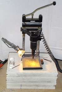
To obtain acceptable accuracy, it is necessary to properly organize the workplace, i.e., firstly, to provide illumination of the board during drilling. To do this, you can use a 12V halogen lamp (or 9V to reduce brightness) and attach it to a tripod to be able to choose the position (illuminate the right side). Secondly, raise the work surface about 6" above the height of the table for better visual control of the process. It would be nice to remove the dust (you can use a regular vacuum cleaner), but this is not necessary - accidentally shorting the circuit with a dust particle is a myth. It should be noted, that the dust from fiberglass generated during drilling is very caustic, and if it gets on the skin, it causes skin irritation.Finally, it is very convenient to use the foot switch of the drilling machine during work, especially when changing drills frequently.
Typical hole sizes:
Via holes - 0.8 mm or less
Integrated circuit, resistors, etc. - 0.8 mm.
Large diodes (1N4001) - 1.0 mm;
· Contact blocks, trimmers - from 1.2 to 1.5 mm;
Try to avoid holes with a diameter of less than 0.8 mm. Always keep at least two spare 0.8mm drills as they always break just at the moment when you urgently need to place an order. Drills 1mm and larger are much more reliable, although it would be nice to have spare ones for them. When you need to make two identical boards, you can drill them at the same time to save time. In this case, it is necessary to very carefully drill holes in the center of the pad near each corner of the PCB, and for large boards, holes located close to the center. So, stack the boards on top of each other and drill 0.8mm holes in two opposite corners, then use the pins as pegs to secure the boards against each other.
cutting
If you are mass-producing PP, you will need guillotine shears for cutting (they cost about 150 USD). Conventional saws dull quickly, except for carbide-coated saws, and sawing dust can cause skin irritation. A saw can accidentally damage the protective film and destroy the conductors on the finished board. If you want to use guillotine shears, then be very careful when cutting the board, remember that the blade is very sharp.

If you need to cut the board along a complex contour, then this can be done either by drilling many small holes and breaking off the PCB along the perforations obtained, or using a jigsaw or a small hacksaw, but be prepared to change the blade often. It is practically possible to make a corner cut with guillotine shears, but be very careful.
through plating
When you make a double-sided board, there is a problem of combining elements on the top side of the board. Some components (resistors, surface integrated circuits) are much easier to solder than others (eg a pin capacitor), so the thought is to surface connect only "light" components. And for DIP components, use pins, and it is preferable to use a model with a thick pin, rather than a connector.

Slightly lift the DIP component off the surface of the board and solder a couple of pins from the solder side, making a small hat on the end. Then you need to solder the required components to the top side using reheating, and while soldering, wait until the solder fills the space around the pin (see figure). For very densely packed boards, the layout needs to be well thought out to facilitate soldering of DIP components. After you have finished assembling the board, it is necessary to carry out a two-way quality control of the installation.
For vias, 0.8 mm quick-mount tie pins are used (see figure).
![]()
This is the most affordable way of electrical connection. All you have to do is insert the end of the tool exactly into the hole all the way, and repeat with the other holes. . This setup is very convenient, but expensive ($350). It uses "plate bars" (see picture), which consist of a solder bar with a copper sleeve plated on the outside.Notches are cut on the bushing with an interval of 1.6 mm, corresponding to the thickness of the board. The bar is inserted into the hole using a special applicator. Then the hole is punched with a core, which causes the plated bushing to warp and also pushes the bushing out of the hole. Pads are soldered on each side of the board to attach the sleeve to the pads, then the solder is removed along with the braid.

Fortunately, this system can be used to plate standard 0.8mm holes without purchasing a complete kit. The applicator can be any automatic pencil with a diameter of 0.8 mm, a model of which has a tip similar to the one shown in the figure, which works much better than a real applicator. Metallization of holes should be done before mounting, while the surface of the board is completely flat. The holes must be drilled with a diameter of 0.85 mm, because after metallization, their diameters decrease.

Note that if your program drew the pads the same size as the drill bit, then the holes could extend beyond the pads, causing the board to malfunction. Ideally, the contact pad extends beyond the hole by 0.5 mm.
Hole plating based on graphite

The second option for obtaining conductivity through holes is metallization with graphite, followed by galvanic copper deposition. After drilling, the surface of the board is covered with an aerosol solution containing fine particles of graphite, which is then pressed into the holes with a squeegee (scraper or spatula). You can use the CRAMOLIN "GRAPHITE" aerosol. This aerosol is widely used in electroforming and other electroplating processes, as well as in obtaining conductive coatings in radio electronics. If the base is a highly volatile substance, then it is necessary to immediately shake the board in a direction perpendicular to the plane of the board, so that excess paste is removed from the holes before the base evaporates. Excess graphite from the surface is removed with a solvent or mechanically - by grinding. It should be noted that the size of the resulting hole can be 0.2 mm smaller than the original diameter. Dirty holes can be cleared with a needle or otherwise. In addition to aerosols, colloidal solutions of graphite can be used. Next, copper is deposited on the conductive cylindrical surfaces of the holes.

The galvanic deposition process is well developed and widely described in the literature. The installation for this operation is a container filled with an electrolyte solution (saturated solution of Cu 2 SO 4 + 10% solution of H 2 SO 4), into which copper electrodes and a workpiece are lowered. A potential difference is created between the electrodes and the workpiece, which should provide a current density of not more than 3 amperes per square decimeter of the workpiece surface. The high current density makes it possible to achieve high copper deposition rates. So, for deposition on a workpiece with a thickness of 1.5 mm, it is necessary to deposit up to 25 microns of copper; at such a density, this process takes a little more than half an hour. To intensify the process, various additives can be added to the electrolyte solution, and the liquid can be subjected to mechanical mixing, bubbling, etc. If copper is applied unevenly to the surface, the workpiece can be polished. The process of metallization with graphite is usually used in subtractive technology, i.e. before applying the photoresist.
Any paste left before applying the copper reduces the free volume of the hole and gives the hole an irregular shape, which complicates further mounting of components. A more reliable method of removing conductive paste residue is by vacuuming or purging with overpressure.
Photomask formation
You need to produce a positive (ie black = copper) translucent photomask film. You will never make a really good PCB without a quality photomask, so this operation is of great importance. It is very important to have a clear andextremely opaqueimage of the PCB topology.
Today and in the future, the photomask will be formed using computer programs of the family or graphic packages suitable for this purpose. In this paper, we will not discuss the advantages of the software, we will only say that you can use any software products, but it is absolutely necessary that the program prints holes located in the center of the pad, used as markers in the subsequent drilling operation. It is almost impossible to manually drill holes without these guidelines. If you want to use general purpose CAD or graphic packages, then in the program settings, specify pads either as an object containing a black filled area with a white concentric circle of smaller diameter on its surface, or as an unfilled circle, setting a large line thickness first (i.e. .black ring).
Once we have determined the location of the contact pads and the types of lines, we set the recommended minimum dimensions:
- drill diameter - (1 mil = 1/1000 inch) 0.8 mm You can make PCB with smaller through holes, but it will be much more difficult.
- pads for normal components and DIL LCS: 65 mil round or square pads with a hole diameter of 0.8 mm.
- line width - 12.5 mils, if you need, you can get 10 mils.
- space between centers of 12.5 mil wide tracks - 25 mils (maybe slightly less if printer model allows).

It is necessary to take care of the correct diagonal connection of the tracks on the cut corners(mesh - 25 mil, track width - 12.5 mil).
The photomask must be printed in such a way that when exposed, the side on which the ink is applied is turned towards the surface of the PCB, in order to ensure a minimum gap between the image and the PCB. In practice, this means that the top side of the double-sided PCB must be printed in a mirror image.
The quality of a photomask is highly dependent on both the output device and the material of the photomask, as well as factors that we will discuss next.
Photomask material
This is not about using a photomask of medium transparency - since a translucent one will be enough for ultraviolet radiation, this is not essential, because. for less transparent material, the exposure time increases quite a bit. Line legibility, black area opacity and toner/ink drying speed are much more important. Possible alternatives when printing a photomask:
Transparent acetate film (OHP)- this may seem like the most obvious alternative, but this replacement can be costly. The material tends to bend or distort when heated by the laser printer, and the toner/ink may crack and flake off easily. NOT RECOMMENDED
Polyester Drawing Film- good but expensive, excellent dimensional stability. Rough surface holds ink or toner well. When using a laser printer, it is necessary to take a thick film, because. when heated, a thin film is subject to warpage. But even thick film can be deformed by some printers. Not recommended, but possible.
Tracing paper. Take the maximum thickness that you can find - at least 90 grams per square meter. meter (if you take it thinner, it can warp), 120 grams per sq. a meter would be even better, but harder to find. It is inexpensive and easily available in offices. Tracing paper has good permeability to ultraviolet radiation and is close to the drawing film in terms of its ability to hold ink, and even surpasses it in its properties not to be distorted when heated.
output device
Pen plotters- painstaking and slow. You will need to use expensive polyester drawing film (tracing paper is not good, because the ink is applied in single lines) and special inks. The pen will have to be cleaned periodically, because. it gets dirty easily. NOT RECOMMENDED.
Inkjet printers- the main problem when using - to achieve the necessary opacity. These printers are so cheap that they are certainly worth a try, but their print quality is not comparable to that of laser printers. You can also try to print on paper first, and then use a good copier to transfer the image to tracing paper.
Typesetters- for the best quality of the photomask, a Postscript or PDF file is created and sent to a DTP or compositor. A photomask made in this way will have a resolution of at least 2400DPI, absolute opacity of the black areas, and perfect image sharpness. The cost is usually given for one page, excluding the area used, ie. if you can replicate copies of the PCB, or put both sides of the PCB on the same page, you'll save money. On such devices, you can also make a large board, the format of which is not supported by your printer.
Laser printers- Easily provide the best resolution, affordable and fast. The printer used must have a resolution of at least 600dpi for all PCBs. we need to make 40 strips per inch. 300DPI will not be able to divide an inch by 40 unlike 600DPI.
It is also important to note that the printer produces good black prints with no toner blotches. If you are planning to buy a PCB printer, then you first need to test this model on a regular sheet of paper. Even the best laser printers may not completely cover large areas, but this is not a problem if thin lines are printed.
When using tracing paper or drawing film, you must have a manual for loading paper into the printer and correctly change the film in order to avoid jamming the equipment. Remember that in the production of small PCBs, to save film or tracing paper, you can cut the sheets in half or to the desired size (for example, cut A4 to get A5).
Some laser printers print with poor accuracy, but since any error is linear, it can be compensated for by scaling the data when printed.
Photoresist
It is best to use FR4 fiberglass already with film resist applied. Otherwise, you will have to cover the workpiece yourself. You don't need a dark room or dim lighting, just avoid direct sunlight by minimizing excess light and develop directly after UV exposure.
Liquid photoresists are rarely used, which are applied by spraying and cover copper with a thin film. I wouldn't recommend using them unless you have the conditions to get a very clean surface or want a low resolution PCB.
Exposure
The photoresist-coated board must be exposed to ultraviolet light through a photomask using a UV machine.
When exposed, standard fluorescent lamps and UV cameras can be used. For a small PCB, two or four 8W 12" bulbs will suffice, for larger ones (A3) four 15" 15W bulbs are ideal. To determine the distance from the glass to the lamp during exposure, place a sheet of tracing paper on the glass and adjust the distance to obtain the desired level of illumination of the paper surface. The UV lamps you need are sold either as replacement parts for medical installations or "black light" lamps for disco lighting. They are colored white or sometimes black/blue and glow with a violet light that makes the paper fluorescent (it glows brightly). DO NOT use short wavelength UV lamps such as erasable ROM or germicidal lamps that have clear glass. They emit short wavelength UV radiation which can cause skin and eye damage and are not suitable for PP production.

The exposure setting can be equipped with a timer that displays the duration of exposure to radiation on the PP, the limit of its measurement should be from 2 to 10 minutes in 30 s increments. It would be nice to provide the timer with an audible signal that indicates the end of the exposure time. It would be ideal to use a mechanical or electronic microwave timer.
You will have to experiment to find the required exposure time. Try exposing every 30s, starting at 20 seconds and ending at 10 minutes. Develop the PP and compare the obtained permits. Note that overexposure produces a better image than underexposure.
So, for exposure of one-sided PCB, turn the photomask with the printed side up on the installation glass, remove the protective film and place the PCB with the sensitive side down on top of the photomask. The PCB should be pressed against the glass to get the minimum gap for the best resolution. This can be achieved either by placing a weight on the surface of the PCB or by attaching a hinged cover with a rubber seal to the UV unit that presses the PCB against the glass. In some installations, for better contact, the PCB is fixed by creating a vacuum under the cap using a small vacuum pump.
When exposing a double-sided board, the side of the photomask with toner (rougher) is applied to the solder side of the PP normally, and to the opposite side (where the components will be placed) - mirrored. After placing the photomasks print side by side and aligning them, check that all areas of the film match. To do this, it is convenient to use a table with backlight, but it can be replaced by ordinary daylight if you combine photomasks on the window surface. If the coordinate accuracy was lost during printing, this may lead to misregistration of the image with holes; try to align the films by the average error value, making sure that the vias do not extend beyond the edges of the pads. After the photomasks are connected and correctly aligned, attach them to the PCB surface with adhesive tape in two places on opposite sides of the sheet (if the board is large, then on 3 sides) at a distance of 10 mm from the edge of the plate. Leaving a gap between the paper clips and the edge of the PCB is important, because this will prevent damage to the edge of the image. Use the smallest size paper clips you can find so that the thickness of the paper clip is not much thicker than the PP.
Expose each side of the PCB in turn. After irradiating the PCB, you will be able to see an image of the topology on the photoresist film.
Finally, it can be noted that a short exposure of the radiation to the eyes is not harmful, but a person may feel discomfort, especially when using powerful lamps. For the installation frame it is better to use glass, not plastic, because. it is more rigid and less prone to cracking on contact.
It is possible to combine UV lamps and white light tubes. If you have many orders for the production of double-sided boards, then it would be cheaper to purchase a double-sided exposure setup, where the PCBs are placed between two light sources, and both sides of the PCB are exposed to radiation at the same time.
Manifestation
The main thing to say about this operation - DO NOT USE SODIUM HYDROXIDE when developing photoresist. This substance is completely unsuitable for the manifestation of PP - in addition to the causticity of the solution, its disadvantages include strong sensitivity to changes in temperature and concentration, as well as instability. This substance is too weak to develop the entire image and too strong to dissolve the photoresist. Those. it is impossible to get an acceptable result with this solution, especially if you set up your laboratory in a room with frequent temperature changes (garage, shed, etc.).
Much better as a developer is a solution made on the basis of silicic acid ester, which is sold as a liquid concentrate. Its chemical composition is Na 2 SiO 3 * 5H 2 O. This substance has a huge number of advantages. The most important is that it is very difficult to overexpose PP in it. You can leave the PP for exactly a non-fixed time. This also means that it almost does not change its properties with temperature changes - there is no risk of decomposition with increasing temperature. This solution also has a very long shelf life, and its concentration remains constant for at least a couple of years.
The absence of the problem of overexposure in the solution will allow you to increase its concentration to reduce the time of development of PP. It is recommended to mix 1 part concentrate with 180 parts water, i.e. 200 ml of water contains just over 1.7 g. silicate, but it is possible to make a more concentrated mixture so that the image develops in about 5 seconds without the risk of surface destruction during overexposure, if sodium silicate cannot be obtained, sodium carbonate or potassium carbonate (Na 2 CO 3) can be used.
You can control the development process by immersing the PCB in ferric chloride for a very short time - the copper will immediately fade, and the shape of the lines of the image can be discerned. If shiny areas remain or the gaps between the lines are blurry, wash the board and soak in the developing solution for a few more seconds. Underexposed PP may leave a thin layer of resist not removed by solvent. To remove film residue, gently rub the PCB with a paper towel that is rough enough to remove the photoresist without damaging the conductors.
You can use either a photolithographic developing tank or a vertical developing tank - the bath is convenient in that it allows you to control the development process without removing the PP from the solution. You will not need heated baths or tanks if the temperature of the solution is maintained at least 15 degrees.
Another recipe for developing solution: Take 200 ml of liquid glass, add 800 ml of distilled water and stir. Then add 400 g of sodium hydroxide to this mixture.
Precautions: Never handle solid sodium hydroxide with your hands, use gloves. When sodium hydroxide is dissolved in water, a large amount of heat is released, so it must be dissolved in small portions. If the solution has become too hot, then allow it to cool before adding another portion of the powder. The solution is very caustic and therefore protective goggles must be worn when working with it. Liquid glass is also known as "sodium silicate solution" and "egg conservator". It is used to clean drainpipes and is sold at any hardware store. This solution cannot be made by simply dissolving solid sodium silicate. The developing solution described above has the same intensity as the concentrate, and therefore it must be diluted - 1 part concentrate with 4-8 parts water, depending on the resist used and temperature.
Etching
Ferric chloride is usually used as an etchant. This is a very harmful substance, but it is easy to obtain and much cheaper than most analogues. Ferric chloride will etch any metal, including stainless steels, so when installing etching equipment, use a plastic or ceramic weir, with plastic screws and screws, and when attaching any materials with bolts, their heads should have a silicon rubber seal. If you have metal pipes, then protect them with plastic (when installing a new drain, it would be ideal to use heat-resistant plastic). Evaporation of the solution is usually not very intensive, but when the baths or tank are not in use, it is better to cover them.
It is recommended to use ferric chloride hexahydrate, which has a yellow color and is sold in the form of powder or granules. To obtain a solution, they must be poured with warm water and stirred until completely dissolved. Production can be significantly improved from an environmental point of view by adding a teaspoon of table salt to the solution. Anhydrous iron chloride is sometimes found, which has the appearance of brown-green granules. Avoid using this substance if possible. It can only be used as a last resort, because. when dissolved in water, it releases a large amount of heat. If you still decide to make an etching solution out of it, then in no case do not fill the powder with water. Granules must be added very carefully and gradually to the water. If the resulting ferric chloride solution does not completely etch the resist, then try adding a small amount of hydrochloric acid and leave it for 1-2 days.
All manipulations with solutions must be carried out very carefully. Do not allow splashing of both types of etchants, because. when they are mixed, a small explosion may occur, causing the liquid to splash out of the container and may get into the eyes or on clothing, which is dangerous. Therefore, wear gloves and goggles while working and immediately wash off any drops that come into contact with the skin.
If you are producing PCB on a professional basis where time is money, you can use heated pickling pots to speed up the process. With fresh hot FeCl, PP will be completely etched in 5 minutes at a solution temperature of 30-50 degrees. This results in better edge quality and a more uniform image line width. Instead of using heated baths, you can place the pickling pan in a larger container filled with hot water.
If you are not using a container with air to agitate the solution, you will need to move the board periodically to ensure even etching.
Tinning
The application of tin to the surface of the PP is carried out to facilitate soldering. The metallization operation consists in deposition of a thin layer of tin (no more than 2 microns) on the copper surface.
Surface preparation of PCB is a very important step before the start of plating. First of all, you need to remove the remaining photoresist, for which you can use special cleaning solutions. The most common solution for stripping the resist is a 3% solution of KOH or NaOH heated to 40-50 degrees. The board is immersed in this solution, and the photoresist peels off the copper surface after a while. After straining, the solution can be reused. Another recipe is with methanol (methyl alcohol). Cleaning is done as follows: holding the PCB (washed and dried) horizontally, drop a few drops of methanol onto the surface, then, slightly tilting the board, try to spread the drops of alcohol over the entire surface. Wait about 10 seconds and wipe the board with a tissue, if the resist remains, repeat the operation again. Then rub the surface of the PCB with a wire cloth (which gives a much better result than sandpaper or abrasive rollers) until you get a shiny surface, wipe with a tissue to remove the particles left by the sponge, and immediately place the board in the tinning solution. Do not touch the board surface with your fingers after cleaning. During the soldering process, the tin can be wetted by the solder melt. It is better to solder with soft solders with acid-free fluxes. It should be noted that if there is a certain period of time between technological operations, then the board must be decapitated in order to remove the formed copper oxide: 2-3 s in a 5% hydrochloric acid solution, followed by rinsing in running water. It is enough to simply carry out chemical tinning, for this the board is dipped into an aqueous solution containing tin chloride. The release of tin on the surface of the copper coating occurs when immersed in a solution of tin salt, in which the copper potential is more electronegative than the coating material. The change in the potential in the desired direction is facilitated by the introduction of a complexing additive into the solution of the tin salt - thiocarbamide (thiourea), alkali metal cyanide. Solutions of this type have the following composition (g/l):
| 1 | 2 | 3 | 4 | 5 | |
| Tin chloride SnCl 2 *2H 2 O | 5.5 | 5-8 | 4 | 20 | 10 |
| Thiocarbamide CS(NH 2) 2 | 50 | 35-50 | - | - | - |
| Sulfuric acid H 2 SO 4 | - | 30-40 | - | - | - |
| KCN | - | - | 50 | - | - |
| Tartaric acid C 4 H 6 O 6 | 35 | - | - | - | - |
| NaOH | - | 6 | - | - | - |
| Sodium lactate | - | - | - | 200 | - |
| Ammonium aluminum sulphate (ammonium alum) | - | - | - | - | 300 |
| Temperature, Сo | 60-70 | 50-60 | 18-25 | 18-25 | 18-25 |
Among the above, solutions 1 and 2 are the most common. Attention! A solution based on potassium cyanide is extremely poisonous!
Sometimes, as a surfactant for 1 solution, it is proposed to use the Progress detergent in an amount of 1 ml / l. Adding 2-3 g/l of bismuth nitrate to solution 2 leads to the precipitation of an alloy containing up to 1.5% bismuth, which improves the solderability of the coating and keeps it for several months. To preserve the surface, aerosol sprays based on fluxing compositions are used. After drying, the varnish applied to the surface of the workpiece forms a strong, smooth film that prevents oxidation. One popular such substance is "SOLDERLAC" from Cramolin. The subsequent soldering passes directly on the processed surface without additional removal of a varnish. In especially critical cases of soldering, the varnish can be removed with an alcohol solution.
Artificial tinning solutions deteriorate over time, especially when exposed to air. Therefore, if you do not regularly have large orders, then try to immediately prepare a small amount of solution, sufficient for tinning the required amount of PP, store the rest of the solution in a closed container (it is ideal to use one of the bottles used in the photo that does not let air through). It is also necessary to protect the solution from contaminants, which can greatly degrade the quality of the substance. Thoroughly clean and dry the workpiece before each process step. You must have a special tray and tongs for this purpose. Tools should also be thoroughly cleaned after use.
The most popular and simple melt for tinning is the fusible alloy - "Rose" (tin - 25%, lead - 25%, bismuth - 50%), the melting point of which is 130 C o. The board is placed with tongs under the level of the liquid melt for 5-10 s, and when removed, it is checked whether all copper surfaces are evenly covered. If necessary, the operation is repeated. Immediately after removing the board from the melt, it is removed either with a rubber squeegee or by sharp shaking in the direction perpendicular to the plane of the board, holding it in the clamp. Another way to remove residues of the Rose alloy is to heat it in an oven and shake it. The operation can be repeated to achieve a mono-thick coating. To prevent oxidation of the hot melt, nitroglycerin is added to the solution so that its level covers the melt by 10 mm. After the operation, the board is washed from glycerin in running water.
Attention! These operations involve working with installations and materials that are under the influence of high temperature, therefore, to prevent burns, it is necessary to use protective gloves, goggles and aprons. The tin-lead tinning operation proceeds similarly, but the higher melt temperature limits the scope of this method in handicraft production.
Three-tank plant: heated pickling bath, bubbling bath and developing tray. As a guaranteed minimum: an pickling bath and a container for rinsing boards. Photo trays can be used for developing and tinning boards.
- A set of tinning trays of various sizes
- Guillotine for PP or small guillotine shears.
- The drilling machine, with a foot pedal of inclusion.
If you cannot get a wash bath, you can use a hand sprayer to wash the boards (for example, to water flowers).
That's it. We wish you to successfully master this technique and get excellent results every time.
Very often, in the process of technical creativity, it is necessary to manufacture printed circuit boards for mounting electronic circuits. And now I will talk about one of the most, in my opinion, advanced methods for manufacturing printed circuit boards using a laser printer and an iron. We live in the 21st century, so we will make our work easier by using a computer.
Step 1. Board design
We will design a printed circuit board in a specialized program. For example, in the program sprint Layout 4.

Step 2. Printing the board pattern
After that, we need to print the board drawing. To do this, we will do the following:
- In the printer settings, turn off all the toner saving options, and if there is an appropriate regulator, set the maximum saturation.
- Let's take an A4 sheet from some unnecessary magazine. The paper should be coated and preferably a minimum of drawing on it.
- We will print the printed circuit board pattern on coated paper in a mirror image. It is better to have several copies at once.

Step 3Cleaning the Board
Let's put the printed sheet aside for now and start preparing the board. Foiled getinaks, foiled textolite can serve as the starting material for the board. During long-term storage, copper foil becomes covered with a film of oxides, which can interfere with etching. So let's start preparing the board. With fine sandpaper, we peel off the oxide film from the board. Don't be too zealous, the foil is thin. Ideally, the board after stripping should shine.

Step 4 Degreasing the Board
After stripping, rinse the board with running water. After that, you need to degrease the board in order for the toner to stick better. You can degrease with any household detergent, or by washing with an organic solvent (for example, gasoline or acetone)

Step 5. Transferring the drawing to the board
After that, using an iron, we transfer the drawing from the sheet to the board. We put the printout with a pattern on the board and start ironing with a hot iron, evenly heating the entire board. The toner will start to melt and stick to the board. The time and effort of warming up is selected experimentally. It is necessary that the toner does not spread, but it is also necessary that it is all welded.

Step 6. Cleaning the board from paper
After the board with the piece of paper stuck to it cools down, we wet it and roll it with our fingers under a stream of water. Wet paper will clump, and adhered toner will remain in place. The toner is quite durable and is difficult to scrape off with a fingernail.

Step 7 Etching the Board
Etching of printed circuit boards is best done in ferric chloride (III) Fe Cl 3. This reagent is sold at any radio parts store and is inexpensive. Immerse the board in the solution and wait. The etching process depends on the freshness of the solution, its concentration, etc. It can take from 10 minutes to an hour or more. The process can be accelerated by shaking the bath with the solution.

The end of the process is determined visually - when all unprotected copper is etched.

The toner is washed off with acetone.

Step 8: Drill holes
Drilling is usually carried out with a small motor with a collet chuck (all this is in the radio parts store). Drill diameter for conventional elements 0.8 mm. If necessary, holes are drilled with a large diameter drill.
What is a printed circuit boardA printed circuit board (English printed circuit board, PCB, or printed wiring board, PWB) is a dielectric plate, on the surface and / or in the volume of which electrically conductive circuits of an electronic circuit are formed. The printed circuit board is designed for electrical and mechanical connection of various electronic components. Electronic components on a printed circuit board are connected with their leads to the elements of the conductive pattern, usually by soldering.
In contrast to surface mounting, on a printed circuit board, the electrically conductive pattern is made of foil, entirely located on a solid insulating base. The printed circuit board contains mounting holes and pads for mounting pin or planar components. In addition, printed circuit boards have vias for electrical connection of foil sections located on different layers of the board. From the outside, the board is usually coated with a protective coating (“solder mask”) and markings (an auxiliary figure and text according to the design documentation).
Depending on the number of layers with an electrically conductive pattern, printed circuit boards are divided into:
single-sided (SPP): there is only one layer of foil glued to one side of the dielectric sheet.
double-sided (DPP): two layers of foil.
multilayer (MPP): foil not only on two sides of the board, but also in the inner layers of the dielectric. Multilayer printed circuit boards are obtained by gluing several single or double sided boards together.
As the complexity of the designed devices and the density of mounting increase, the number of layers on the boards increases.
The basis of the printed circuit board is a dielectric, the most commonly used materials are fiberglass, getinaks. Also, a metal base coated with a dielectric (for example, anodized aluminum) can serve as the basis for printed circuit boards; copper foil tracks are applied over the dielectric. Such printed circuit boards are used in power electronics for efficient heat removal from electronic components. In this case, the metal base of the board is attached to the radiator. As a material for printed circuit boards operating in the microwave range and at temperatures up to 260 ° C, fluoroplastic reinforced with glass fabric (for example, FAF-4D) and ceramics are used. Flexible boards are made from polyimide materials such as Kapton.
What material will we use for the manufacture of boards
The most common, affordable materials for the manufacture of circuit boards are Getinaks and Steklotekstolit. Getinax paper impregnated with bakelite varnish, fiberglass textolite with epoxy. We will definitely use fiberglass!
Foiled fiberglass is sheets made on the basis of glass fabrics impregnated with a binder based on epoxy resins and lined on both sides with copper electrolytic galvanic-resistant foil 35 microns thick. The maximum allowable temperature is from -60ºС to +105ºС. It has very high mechanical and electrical insulating properties, lends itself well to machining by cutting, drilling, stamping.
Fiberglass is mainly used one or two-sided with a thickness of 1.5mm and with copper foil with a thickness of 35μm or 18μm. We will use a 0.8mm thick single-sided fiberglass with a 35µm thick foil (why will be discussed in detail later).

Methods for making printed circuit boards at home
Boards can be manufactured chemically and mechanically.
With the chemical method, in those places where there should be tracks (drawing) on the board, a protective composition (lacquer, toner, paint, etc.) is applied to the foil. Next, the board is immersed in a special solution (ferric chloride, hydrogen peroxide, and others), which "corrodes" the copper foil, but does not affect the protective composition. As a result, copper remains under the protective composition. The protective composition is subsequently removed with a solvent and the finished board remains.
The mechanical method uses a scalpel (for manual production) or a milling machine. A special cutter makes grooves on the foil, eventually leaving islands with foil - the necessary pattern.
Milling machines are quite expensive, as well as the cutters themselves are expensive and have a small resource. So, we will not use this method.

The simplest chemical method is manual. With a risograph varnish, tracks are drawn on the board and then we etch with a solution. This method does not allow making complex boards with very thin traces - so this is not our case either.

The next method for making boards is with a photoresist. This is a very common technology (boards are made by this method at the factory) and it is often used at home. There are a lot of articles and methods for manufacturing boards using this technology on the Internet. It gives very good and repeatable results. However, this is also not our option. The main reason is rather expensive materials (photoresist, which also deteriorates over time), as well as additional tools (UV lamp, laminator). Of course, if you have a bulk production of boards at home - then the photoresist is out of competition - we recommend mastering it. It is also worth noting that the equipment and technology of photoresist allows the production of silk-screen printing and protective masks on circuit boards.

With the advent of laser printers, radio amateurs began to actively use them for the manufacture of circuit boards. As you know, a laser printer uses "toner" to print. This is a special powder that sinters under temperature and sticks to paper - as a result, a pattern is obtained. The toner is resistant to various chemicals, which allows it to be used as a protective coating on the copper surface.
So, our method is to transfer the toner from the paper to the surface of the copper foil and then etch the board with a special solution to obtain a pattern.
Due to its ease of use, this method has earned a very wide distribution in amateur radio. If you type in Yandex or Google how to transfer the toner from paper to the board, you will immediately find such a term as "LUT" - laser ironing technology. Boards using this technology are made as follows: a pattern of tracks is printed in a mirror version, paper is applied to the board with a pattern to copper, we iron this paper on top, the toner softens and sticks to the board. The paper is further soaked in water and the board is ready.

There are "a million" articles on the Internet about how to make a board using this technology. But this technology has many disadvantages that require direct hands and a very long attachment to it. That is, you have to feel it. Payments do not come out the first time, they are obtained every other time. There are many improvements - to use a laminator (with alteration - in the usual one there is not enough temperature), which allow to achieve very good results. There are even methods for building special heat presses, but all this again requires special equipment. The main disadvantages of LUT technology:
overheating - the tracks spread out - become wider
underheating - tracks remain on paper
the paper is “cooked” to the board - even when it is soaked, it is difficult to leave - as a result, the toner may be damaged. There is a lot of information on the Internet about which paper to choose.
Porous toner - after removing the paper, micropores remain in the toner - the board is also etched through them - corroded tracks are obtained
repeatability of the result - excellent today, bad tomorrow, then good - it is very difficult to achieve a stable result - you need a strictly constant toner warm-up temperature, you need a stable board pressure.
By the way, this method did not work for me to make a board. Tried to do both on magazines and on coated paper. As a result, he even spoiled the boards - copper swelled from overheating.
For some reason, there is undeservedly little information on the Internet about another method of toner transfer - the method of cold chemical transfer. It is based on the fact that toner does not dissolve with alcohol, but with acetone. As a result, if you choose such a mixture of acetone and alcohol, which will only soften the toner, then it can be “re-pasted” onto the board from paper. I really liked this method and immediately paid off - the first board was ready. However, as it turned out later, I could not find detailed information anywhere that would give a 100% result. We need a method by which even a child could make a payment. But for the second time, the payment did not work out, then again it took a long time to select the necessary ingredients.
As a result, after a long time, a sequence of actions was developed, all components were selected that give, if not 100% then 95% of a good result. And most importantly, the process is so simple that the child can make the payment completely on his own. This is the method we will use. (Of course, it can be further improved to the ideal - if it works out better for you, then write). The advantages of this method:
all reagents are inexpensive, available and safe
no additional tools are needed (irons, lamps, laminators - nothing, although not - you need a pan)
there is no way to spoil the board - the board does not heat up at all
paper moves away by itself - you can see the result of the transfer of toner - where the transfer did not come out
there are no pores in the toner (they are sealed with paper) - accordingly, there are no mordants
do 1-2-3-4-5 and always get the same result - almost 100% repeatability
Before we start, let's see what boards we need, and what we can do at home with this method.
Basic requirements for manufactured boards
We will make devices on microcontrollers, using modern sensors and microcircuits. Microcircuits are getting smaller and smaller. Accordingly, the following requirements must be met:
boards must be two-sided (as a rule, it is very difficult to separate a single-sided board, it is rather difficult to make four-layer boards at home, microcontrollers need a ground layer to protect against interference)
the tracks should be 0.2mm thick - this size is quite enough - 0.1mm would be even better - but there is a possibility of pickling, track departure during soldering
the gaps between the tracks - 0.2mm - this is enough for almost all circuits. Reducing the gap to 0.1mm is fraught with merging of tracks and difficulty in monitoring the board for short circuits.
We will not use protective masks, and also do silk-screening - this will complicate the production, and if you are making the board for yourself, then this is not necessary. Again, there is a lot of information on the Internet on this topic, and if you wish, you can make a “marafet” yourself.
We will not tinker with the boards, this is also not necessary (unless you are making a device for 100 years). For protection, we will use varnish. Our main goal is to quickly, efficiently, cheaply make a board for the device at home.
This is what the finished board looks like. made by our method - tracks 0.25 and 0.3, distances 0.2

How to make a double-sided board from 2 single-sided
One of the problems with making double-sided boards is aligning the sides so that the vias line up. Usually a "sandwich" is made for this. 2 sides are printed on a sheet of paper at once. The sheet is bent in half, the sides are precisely aligned with the help of special marks. Double-sided textolite is inserted inside. With the LUT method, such a sandwich is ironed and a double-sided board is obtained.
However, in the cold transfer toner method, the transfer itself is carried out with the help of a liquid. And therefore it is very difficult to organize the process of wetting one side simultaneously with the other side. Of course, this can also be done, but with the help of a special device - a mini press (vice). Thick sheets of paper are taken - which absorb the toner transfer liquid. The sheets are wetted so that the liquid does not drip and the sheet holds its shape. And then a “sandwich” is made - a wetted sheet, a sheet of toilet paper to absorb excess liquid, a sheet with a pattern, a double-sided board, a sheet with a pattern, a sheet of toilet paper, again a wetted sheet. All this is clamped vertically in a vise. But we will not do this, we will do it easier.
A very good idea slipped through the board manufacturing forums - what a problem it is to make a double-sided board - we take a knife and cut the textolite in half. Since fiberglass is a puff material, it is not difficult to do this with a certain skill:

As a result, from one double-sided board with a thickness of 1.5 mm, we get two one-sided halves.

Next, we make two boards, drill and that's it - they are perfectly aligned. It was not always possible to cut the textolite evenly, and as a result, the idea came up to immediately use a thin one-sided textolite with a thickness of 0.8 mm. Then you can not glue the two halves, they will be held by soldered jumpers in vias, buttons, connectors. But if necessary, you can glue it with epoxy glue without any problems.
The main advantages of this trip:
Textolite with a thickness of 0.8 mm is easily cut with scissors on paper! In any shape, that is, it is very easy to cut to fit the body.
Thin textolite - transparent - by shining a lantern from below, you can easily check the correctness of all tracks, short circuits, breaks.
Soldering one side is easier - the components on the other side do not interfere and you can easily control the soldering of microcircuit pins - you can connect the sides at the very end
You need to drill twice as many holes and the holes may slightly misalign.
The rigidity of the structure is slightly lost if you do not glue the boards, and gluing is not very convenient
One-sided fiberglass 0.8mm thick is difficult to buy, mostly 1.5mm is sold, but if you couldn’t get it, you can cut a thicker textolite with a knife.
Let's move on to the details.
Necessary tools and chemistry
We will need the following ingredients:


Now that all this is there, let's do it step by step.
1. Layout of board layers on a sheet of paper for printing using InkScape

Automatic collet set:

We recommend the first option - it is cheaper. Next, you need to solder wires and a switch to the motor (preferably a button). It is better to place the button on the body, so that it is more convenient to quickly turn the motor on and off. It remains to choose a power supply, you can take any power supply for 7-12V with a current of 1A (or less), if there is no such power supply, then charging via USB at 1-2A or a Kron battery may be suitable (you just need to try - not all chargers like motors, the motor may not start).
The drill is ready, you can drill. But it is only necessary to drill strictly at an angle of 90 degrees. You can build a mini machine - there are various schemes on the Internet:

But there is an easier solution.
Drill jig
To drill exactly at 90 degrees, it is enough to make a drilling jig. We'll do something like this:

It is very easy to make it. We take a square of any plastic. We put our drill on a table or other flat surface. And we drill a hole in the plastic with the right drill. It is important to ensure a smooth horizontal displacement of the drill. You can lean the motor against a wall or rail and plastic too. Next, use a large drill to drill a hole for the collet. On the reverse side, drill or cut off a piece of plastic so that the drill can be seen. A non-slip surface can be glued to the bottom - paper or an elastic band. Such a conductor must be made for each drill. This will ensure perfectly accurate drilling!
This option is also suitable, cut off the top part of the plastic and cut off the corner from the bottom.

Here is how drilling is done with it:

We clamp the drill so that it sticks out 2-3 mm when the collet is fully immersed. We put the drill in the place where it is necessary to drill (when etching the board, we will have a mark where to drill in the form of a mini hole in copper - in Kicad we specially set a checkbox for this, so that the drill will get up there by itself), press the conductor and turn on the motor - the hole ready. For illumination, you can use a flashlight by placing it on the table.
As we wrote earlier, you can only drill holes on one side - where the tracks fit - the second half can be drilled without a jig along the first guide hole. This saves some power.
8. Tinning board
Why tin boards - mainly to protect copper from corrosion. The main disadvantage of tinning is overheating of the board, possible damage to the tracks. If you do not have a soldering station - definitely - do not tin the board! If it is, then the risk is minimal.
It is possible to tin the board with ROSE alloy in boiling water, but it is expensive and difficult to obtain. It is better to tin with ordinary solder. To do this qualitatively, a very thin layer must be made a simple device. We take a piece of braid for soldering parts and put it on the sting, fasten it with a wire to the sting so that it does not come off:
We cover the board with a flux - for example, LTI120 and a braid too. Now we collect tin into the braid and we drive it along the board (we paint it) - we get an excellent result. But with use, the braid falls apart and copper fibers begin to remain on the board - they must be removed, otherwise there will be a short circuit! It is very easy to see this by shining a flashlight on the back of the board. With this method, it is good to use either a powerful soldering iron (60 watts) or ROSE alloy.
As a result, it is better not to tin the boards, but to varnish at the very end - for example, PLASTIC 70, or a simple acrylic varnish bought in auto parts KU-9004:

Fine tuning of the toner transfer method
There are two points in the method that are amenable to tuning, and may not work right away. To set them up, you need to make a test board in Kicad, tracks in a square spiral of different thicknesses, from 0.3 to 0.1 mm and at different intervals, from 0.3 to 0.1 mm. It is better to immediately print several of these samples on one sheet and adjust.
Possible issues we will be fixing:
1) tracks can change geometry - spread, become wider, usually not very much, up to 0.1mm - but this is not good
2) the toner may not adhere well to the board, move away when removing the paper, it may not adhere well to the board
The first and second problems are interrelated. I solve the first, you come to the second. We must find a compromise.
The tracks can spread for two reasons - too much clamping weight, too much acetone in the composition of the resulting liquid. First of all, you need to try to reduce the load. The minimum load is about 800g, you should not reduce it below. Accordingly, we put the load without any pressure - we just put it on top and that's it. Be sure to have 2-3 layers of toilet paper for good absorption of excess solution. You must ensure that after removing the load, the paper should be white, without purple smudges. Such smudges indicate a strong melting of the toner. If it was not possible to adjust the load with the load, the tracks still blur, then we increase the proportion of nail polish remover in the solution. Can be increased to 3 parts liquid and 1 part acetone.
The second problem, if there is no geometry violation, indicates an insufficient weight of the cargo or a small amount of acetone. Again, it's worth starting with the load. More than 3 kg does not make sense. If the toner still does not adhere well to the board, then you need to increase the amount of acetone.
This problem mostly occurs when you change your nail polish remover. Unfortunately, this is not a permanent and not a pure component, but it was not possible to replace it with another one. I tried to replace it with alcohol, but apparently the mixture is not homogeneous and the toner sticks with some inclusions. Also, nail polish remover may contain acetone, then it will need less. In general, you will need to carry out such tuning once until the liquid runs out.
Board ready
If you do not immediately solder the board, then it must be protected. The easiest way to do this is to coat with alcohol rosin flux. Before soldering, this coating will need to be removed, for example, with isopropyl alcohol.
Alternatives
You can also make a payment:
Additionally, a custom board manufacturing service is now gaining popularity - for example, Easy EDA. If a more complex board is needed (for example, a 4-layer board), then this is the only way out.
When making printed circuit boards at home, the simplest and most common method is the LUT method.
This method is not without drawbacks. If the toner is heated weakly, then it will not stick to the printed circuit board foil, if heated strongly, it will be smeared. It is necessary to select the print quality, if there is a lot of toner, it will be smeared, the tracks, at small intervals, may stick together. It is bad to warm up the printed board, and some of the tracks will not be printed, especially this often happens in the corners of printed circuit boards.
I will tell you about a method for transferring a printed pattern to foil without heating. The drawing will not be smeared, all the toner is transferred from the paper. To do this, you need two cheap chemical components: alcohol and acetone.


Instead of acetone, you can use any other substance that dissolves the toner well.
Alcohol does not react with toner, anyone who has tried to scrub a PCB with it after etching knows this, but it quickly disappears. It is needed in order to dilute the acetone.
Acetone dissolves toner very well and also evaporates quickly. If you try to use it in its pure form, it will smear your drawing, as in the photo.

There will be some kind of mess on the printed circuit board.
In what proportions should acetone and alcohol be mixed?
It will take three parts of acetone and eight parts of alcohol. All this must be mixed and poured into a container with a tight lid. It is important that the container does not dissolve with acetone.
How to use the mixture?
Draw a little of the resulting mixture into a syringe,


Apply it to the future printed circuit board, previously cleaned of oxides and well degreased (this is important) (not on a printout). After that, put your printout on it. You can especially take your time, the mixture does not disappear instantly. Lightly press the paper so that it is completely attached to the board and soaked with the solution,

Wait 10-15 seconds, you will see when the paper is saturated,

After that, press the paper firmly, press the paper strictly perpendicular so that it does not move. Wait another 10-20 seconds. During this time, the toner will react with acetone, become sticky and stick to the board. Blot the remaining liquid with paper towels, wait until the paper dries, then dip the board in water so that the paper gets wet, and peel it off. All the toner will remain on the board, and the paper will be clean. After that, rinse the board from the remnants of acetone. All. You can etch the printed circuit board.
In the photo, I removed the paper without soaking it in water and the toner remained in places.